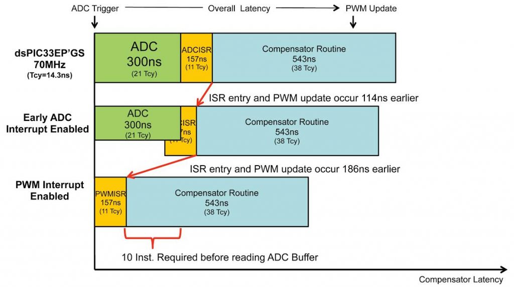
One unique feature about the ADC is the capability to generate the interrupt before conversion completes. This ADC early interrupt feature, when enabled, helps to reduce the interrupt latency from the time the ADC completes conversion to the start of control loop software (interrupt). The maximum selectable early interrupt timing is eight ADC clocks (Tads). At the fastest throughput this reduces the time taken to get into the compensator algorithm by 114ns. This is yet another way to reduce the total latency in the control loop software. See Figure 4 for details on ADC early interrupt.

Another ADC module feature is the inclusion of multiple digital comparators that can be configured to give an interrupt when the converted analog result is outside (or within) a given set of limits. This may not seem like a feature that directly impacts the sampling frequency, but it most definitely can. Fewer MIPS are consumed when software is offloaded from the CPU and only executed in a fault condition. This means that we may be able to increase the sampling rate of the control loop. This is highly software dependent and not all applications may be able to take advantage of this new feature. However, it can reduce the CPU work load when it comes to examples like input voltage and temperature monitoring.
To reduce the time from ADC trigger to control output write back even further the PWM ISR could be used instead of the ADC interrupt service routine (ISR) and the ADC early interrupt feature. In a general use case, the PWM triggers the ADC to start conversion but now it will also generate its own interrupt event at the same time. With the compensator algorithm placed inside the PWM ISR, the software will start executing the compensator algorithm before the current feedback data is available from the ADC. There is roughly 143ns between software execution and completion of the ADC conversion. This means there needs to be a minimum of 10 instructions placed before reading the ADC result buffer when the microcontroller is operating at maximum device frequency. If the compensator algorithm is structured in such a way that this technique can be used, it will reduce the time taken to get into the compensator routine by 45%. See Figure 4 for an early interrupt timing example with PWM interrupt service routine. It is important to note that this method should only be applied with the predictable timing of the dedicated SAR cores.
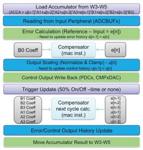
The structure of the compensator algorithm plays an important role in the time it takes to update the control output variable. With the alternate working registers, the algorithm can be written in such a way that the only required computations before updating the control output is to multiply the current error with coefficient B0 and to add that to the accumulated output from the previous cycle. Of course the backward normalization and clamping is still there but this will significantly reduce the control output write back time without requiring a dedicated accumulator. Figure 5 shows an example of how the compensator algorithm can be arranged to achieve the quickest update time. The control output write back time can now occur in less than 300ns upon entering the compensator algorithm. It will become clear how this is useful in the following sections.

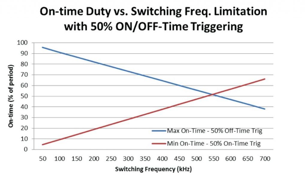
Now let us consider the impact of all these different features on phase erosion. In voltage mode control and average current mode control systems, it is possible to sample the output capacitor voltage or inductor current at 50% of the off-time. Most common approach is to sample at 50% on-time to allow enough time to process the control algorithm before the start of the next PWM cycle. With all the features mentioned above it is easily possible to sample the control feedback signals during the off-time and write back to control output before the start of the next PWM cycle. Figure 6 shows the estimated duty cycle limits for an example implementation across switching frequencies while Figure 7 illustrates a timing diagram of 50% off-time. The increase in phase margin is dependent on duty cycle but if averaged at 50% duty cycle the phase erosion drops by half compared to the 50% on-time measurement.

The dsPIC33EP ‘GS’ devices feature an immediate update mode that when enabled will update the PWM parameters within the current cycle when the special function register (SFR) is also written. This applies to phase, period, deadtime and duty cycle all with a resolution of 1ns. In the 50% off-time scenario, it was mentioned that the control output write back had to occur before the start of the next PWM cycle and this limits what the maximum on time is for a given switching frequency. With immediate updates enabled, this is no longer the case. This feature now allows duty cycle limits and/or switching frequency limits to increase even further which will help in reducing phase margin erosion once again. Figure 7 illustrates the timing for both 50% off-time implementations.

The best case for reducing phase margin erosion is to sample the control feedback signal at 50% on-time while ensuring that the new control output is applied to the trailing edge of current PWM cycle. This implies that the active edge of the PWM duty cycle is being updated based on the output of the compensator that was just called in the same PWM cycle. This would give the best phase margin possible in a digital system. One should note that this is the optimum use case but cannot be implemented in all applications due to limitations with minimum on-time. See Figure 6 for minimum on-time as a percent of the switching period across different switching frequencies. For example, if will take a boost PFC switching at 100kHz, the minimum on-time requirement would be slightly less than 10% of the period. As the minimum duty cycle occurs at the peak of the AC line voltage, at nominal 220V input voltage, the duty cycle requirement is around 22% leaving ample headroom for the immediate update to occur with large variations in the control output. As input voltage increases further, the immediate update will start to look like the end of cycle update and there will be a reduction in phase margin. However, this will occur outside of the nominal conditions. Figure 7 also shows the timing diagram for a 50% on-time trigger use case as compared against the 50% on-time trigger schemes.
An example was carried out using a synchronous buck converter in which all of the techniques discussed in this article where incorporated. The results showed that the sampling rate increased from every other PWM cycle (175kHz) to every PWM cycle (350kHz) without requiring more MIPS, the compensator was written for quick write back to the control output variable, the PWM interrupt was generated for processing the control loop, and 50% on-time with immediate updates was enabled. What was observed was an increase in phase margin of roughly 16 degrees. The loop gain performance started out to be marginally stable with only 46 degrees of phase margin and ended up being very close to an analog counterpart at 62 degrees. The techniques for reducing phase erosion in this paper are not a cure-all; however they are applicable to a wide range of designs and will provide some degree of loop gain enhancements.


