New Technology developments like foldable flexible perovskite LEDs and a core chip for 3D image sensors respectively have been achieved by researchers of the Korea Advanced Institute of Science and Technology (UNIST) and the Ulsan National Institute of Science and Technology (KAIST).
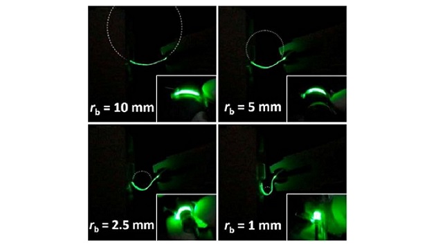
UNIST researchers have developed foldable perovskite LEDs (PeLED) with a transparent material as electrode of the device. A perovskite material as light emitting layer through electricity is used by the PeLED. A flexible silver nanowire and conductive polymers in electrodes were utilized by the researchers, to replace the conventional metal electrode, which increased the PeLED’s flexibility.
Moreover, the polymer electrolytes were also added by the researchers, to enhance the electron mobility for improving device performance. Thus, the new PeLED can achieve 50 percent transparency and remain light emitting with being bended.
Whereas the other research team from KAIST developed a silicon-based optical phased array (OPA) chip for 3D image sensor for applications including the drones, robots and the autonomous vehicles.
KAIST collaborated with the National Nanofab Center in South Korea, to introduce an ultra-small low power OPA device, which controls the direction of light for scanning. The light could be converted into a single wavelength light source by the chip.
The small sized chip helps to make 3D image sensor smaller and can further transmit data wirelessly to the desired direction.

