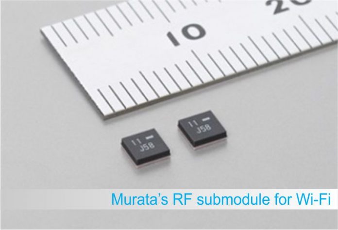
Murata Manufacturing started in April the mass production of RF sub-modules for Wi-Fi. This product uses Murata semiconductor design technology, monolithic ceramic technology, and circuit design technology to reduce the size of the front end circuit in order to incorporate the Wi-Fi function. This enables reduction of the component surface mount area and decreasing of component contact points in comparison to circuits with the former discrete structure. It saves area for customer design, and contributes to design resources and shortens development cycles.
Features
- Compliant with Wi-Fi 2.4G、5GHz IEEE802.11a/b/g/n/ac.
- Incorporates required structural elements such as PA, LNA, RF switch, filter, duplexer and coupler.
- Compatible with Qualcomm Atheros made WCN3990 chip set.
Applications
- Mobile devices such as smartphones and tablet PCs.
Part number
LMFE3NFB-J58
LMFE3NFB-J38
External size
3.0×3.0x0.9max mm
For more information, visit Murata’s website at www.murata.com

