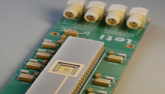
Leti, an institute of CEA, and CEA-IRIG, a fundamental research institute, have created the world’s first quantum integrated circuit that demonstrates the possibility of integrating conventional electronic devices and elements with quantum dots on a CMOS chip.
The chip, fabricated on 28nm FD-SOI process, integrates analog and digital functions (multiplexer, buffer, signal amplifier, oscillator, level converter) that represent future instrumentation needs for the quantum accelerator envisioned in CEA-Leti’s quantum initiative.
Beyond the need to obtain reliable, entangled and coherent quantum bits, or qubits, on silicon, the goal of this work is ultimately to produce electronics capable of routing numerous signals to address a matrix of several hundred qubits. These results also demonstrate CEA-Leti’s know-how in cryogenic instrumentation in FD-SOI technology and can also be used for other non-silicon quantum devices such as superconducting qubits.
The results were presented in a paper, “A 110mK 295μW 28nm FD-SOI CMOS Quantum Integrated Circuit with a 2.8GHz Excitation and nA Current Sensing of an On-chip Double Quantum Dot”, on Feb. 18 at ISSCC 2020 in San Francisco.
“To reach quantum supremacy, quantum computers need >50 logical qubits with Loïck Le Guevel, a lead author of the paper, explained that the quantum integrated circuit is a proof-of-concept circuit merging microelectronics benchmarks and quantum dots operating at sub-Kelvin temperature within a limited power budget.
“It uses all elements required to properly design high-spec state-of-the-art circuits, such as passive elements, resistors and capacitors, transistors for digital operation up to 7Ghz, and transistors for analog operation up to 3Ghz,” he said. “On top of that, we were able to design a double quantum dot in the same semiconductor layer as transistors using a standard fabrication flow. This realization emphasizes that FD-SOI could one day allow circuit designers to use qubit arrays embedded in IP blocks with classic electronics to build custom-made, large-scale quantum silicon processors.”
Le Guevel is a Ph.D. student supervised by Gaël Pillonnet and Louis Jansen in the Quantum Silicon Grenoble research group led by Maud Vinet. In addition to demonstrating a highly sensitive analog current read-out operating at 110mK, 40x lower than competing technologies, within the limited power budget, the researchers demonstrated the possibility of having GHz digital signal generation, and GHz signal analog manipulation.
A quantum dot structure, very similar to the first realization of a spin qubit on a silicon 300mm industrial wafer by the Quantum Silicon Grenoble group, also was fabricated on the same semiconductor layer using industrial-grade design software and common foundry design rules. Despite the close proximity (<1 micrometer) of dissipating high-speed electronics and a sensitive quantum-dot device, quantum effects were preserved and open a path toward an industrially made quantum dot device that will benefit from a higher reproducibility/yield of the silicon CMOS technology.
In the medium-term, the quantum community is focused on noisy intermediate-scale quantum technology (NISQ) that has the potential to outperform classical supercalculators in some specific tasks, such as path optimization, quantum deep learning, neural networks, AI and recommendation systems. This first co-integration together with the recently published performance on silicon-based qubits confirms that silicon is a serious contender, as it allows fast operations while maintain competitive fidelity with controlled process reproducibility on a scalable footprint.
For more information, visit www.leti-cea.com

