Large-area electronics (LAE) is an emerging technology for the electronics device manufacturers, such as printing or large-scale lithography, the process used to create flat panel displays and solar cells. Using LAE processes, engineers could create systems that are large (several square meters squared) and highly flexible; for instance, based on paper or plastic.
Over the past decade or so, many teams worldwide have been working on LAE systems. This has led to the creation of numerous innovative devices, such as large, flexible and sensing artificial skins for robots.
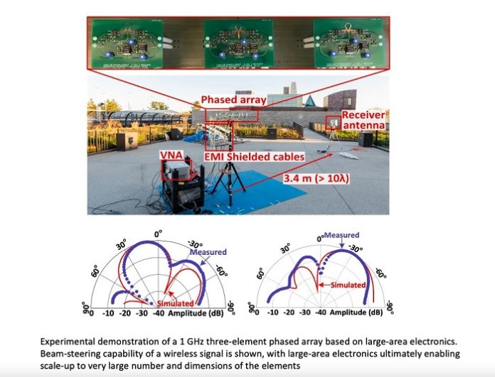
Researchers at Princeton University have recently realized a new wireless system based on LAE technology that can operate at gigahertz frequencies. This system is based on an array of high-speed, self-aligned zinc-oxide thin-film transistors.
“This work started by imagining the new capabilities for electronic systems that could be enabled by LAE, which is a very different technology than what we use to build most electronic devices today (i.e., CMOS chips),” Naveen Verma, one of the researchers who carried out the study.
A key limitation of existing LAE-based devices is that they typically achieve far lower speeds than electronics based on conventional chips. This significantly limits their potential for wireless applications, despite the notable advantages of having wireless systems with a large size and significant flexibility.
“Recent work by us and others has pushed the speed of LAE, with some of our recent devices breaking the gigahertz frequency barrier,” Verma explained. “By combining this with some circuit and architecture co-design, we found that it is now possible to build relevant wireless systems that can take advantage of the unprecedented size and flexible formfactor that LAE offers.”
While creating their system, Verma and his colleagues carefully considered its design, circuitry and architecture. To enhance its speed, they enhanced a metric of basic transistors by over one order of magnitude and then designed circuits that exploited this metric. Finally, they employed architecture-level phase synchronization techniques that did not require components that would reduce the system’s speed.
“This is the exciting part: this very different kind of technology gives really transformative new capabilities, but it requires new ways of thinking about the operation and design,” Verma said. “The notable achievement of our work was the demonstration of a wireless system, namely a phased array, in LAE technology, that directly and significantly benefits from large area.”
The researchers evaluated their LAE device in a series of tests and found that it operated at a frequency of approximately 1GHz. In addition, their system was found to have beamforming capabilities, meaning that it is capable of enhancing wireless communication with targets at specific locations. In the future, their work could thus pave the way towards the realization of LAE systems that are large and flexible, but that can also perform computations rapidly and communicate with other systems via wireless technology.
“Our study suggests that realizing the wireless capabilities of interest with devices of very large physical dimensions is indeed possible,” Verma said. “With basic giga-Hertz LAE devices in-hand and a circuit-/architecture-level understanding of how to utilize these, our focus will now be on exploring different wireless systems to investigate how the unprecedented sizes and formfactors can enable new application and application-level capabilities.”


