Designers of untethered Internet of Things (IoT) devices are constantly on the lookout for better ways to power these devices to minimize downtime across consumer, commercial or industrial applications. Primary batteries need to be constantly monitored, and when they are eventually replaced, they add a significant disposal problem. Rechargeable batteries address the disposal problem, but devices need to be dismounted, recharged, and remounted.
The limitations of traditional approaches have resulted in increased interest in energy harvesting techniques where ambient energy is used to power a device. The problem for designers is that the circuits needed to harvest energy and recharge batteries can add significantly to design complexity, size, and cost.
This article briefly makes the case for the use of energy harvesting in IoT applications and outlines some of the challenges designers face. It then introduces an approach that overcomes these challenges by integrating energy harvesting and battery charge management circuits on a microcontroller (MCU). Using example device solutions and associated evaluation boards from Renesas, the article will show how to apply the approach to effectively eliminate the need for battery replacement in IoT devices.
Why use energy harvesting for IoT?
Energy harvesting is an attractive solution for IoT applications such as low-power wireless sensor systems, where it enables the deployment of completely wire-free devices that require little or no maintenance. Typically, these devices still need a rechargeable battery or supercapacitor to meet peak power demands.
In principle, by harvesting ambient energy, the system can employ a smaller energy storage device and extend its useful life. In turn, the resulting IoT design can potentially fit in a smaller package as long as the energy harvesting functionality adds little to the design’s parts count. In practice, however, the need for additional components to implement energy harvesting frustrates attempts to reduce design footprint.
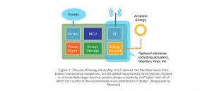
The problem is that an energy harvesting power source typically requires separate devices to harvest ambient energy and ensure proper charge management for an energy storage device like a rechargeable battery or supercapacitor. Added to an already minimalist wireless system design comprising an MCU, sensor, and radio frequency (RF) transceiver, this additional functionality can turn a simple design with few parts into a relatively complex one (Figure 1).
 Minimizing components for IoT designs
To date, many of the various components required for energy harvesting have been integrated into specialized modules and power management integrated circuits (PMICs) like Analog Devices’ LTC3105/LTC3107, Cypress Semiconductor’s S6AE101A, Matrix Industries’ MCRY12-125Q-42DIT, and many others. Such devices provide a regulated voltage rail from a solar cell, thermoelectric generator (TEG), piezoelectric vibration transducer, or other energy source. As such, they can serve as a complete energy harvesting power supply for a basic IoT hardware design. Still, designers need to push the envelope to meet application requirements and retain or achieve competitive advantage.
The Renesas RE01 MCU family helps with these goals as it takes the integration approach further by including an energy harvesting controller (EHC) within the device. In fact, an RE01 MCU can use its built-in EHC to recharge a secondary battery while providing system power to the rest of the device. More than just an energy harvesting device, the RE01 includes its EHC with a 64 megahertz (MHz) Arm® Cortex®-M0+ core, on-chip Flash, a trusted secure intellectual property (TSIP) block, a 14-bit analog-to-digital converter (ADC), timers, and multiple peripheral interfaces (Figure 2).
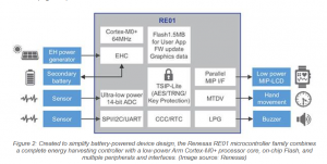 Designed to simplify implementation of battery-powered IoT devices, the RE01 integrates a comprehensive set of relevant peripheral functionality. Along with its ADC and serial interfaces for sensor integration, the device includes a motor driver control circuit (“MTDV” block in Figure 2) able to drive up to three motors; a constant current source able to drive three external light emitting diodes (LEDs); and a low-speed pulse generator (LPG). For display output, the RE01 MCU integrates a graphic accelerator for two-dimensional (2D) image processing as well as a memory-in-pixel (MIP) liquid crystal display (LCD) controller. For real-time control requirements, the MCU also includes a watchdog timer, a real-time clock (RTC) and clock correction circuit (CCC) that maintains clock precision. For software code and data, the RE01 family combines the functionality mentioned above in member devices including the R7F0E015D2CFP (RE01 1500KB) with 1500 Kbytes of Flash, and the R7F0E01182CFM (RE01 256KB) with 256 kilobytes (Kbytes) of Flash.
Along with its functional capabilities, the RE01 MCU provides plenty of options for finding the required balance between performance and power consumption. The MCU can run in multiple operating modes that minimize power consumption by reducing the operating frequency from its maximum 64 MHz rate down to 32.768 kilohertz (kHz) in a low leakage current mode, with intermediate frequencies in normal operating mode of 32 MHz or 2 MHz. In typical operation, the R7F0E015D2CFP RE01 1500KB typically consumes only 35 microamps per megahertz (µA/MHz) active current and only 500 nanoamp (nA) current in standby mode at 1.62 volts. Its 14-bit ADC draws only 4 µA, and Flash programming rewrites need only about 0.6 milliamps (mA). In providing the supply for these normal operations, the RE01 MCU’s EHC integrates an extensive set of capabilities designed to ease implementation of energy harvesting and battery management.
Integrated energy harvesting controller simplifies design
Thanks to its integrated EHC, the RE01 MCUs make implementation of energy harvesting a rather routine operation. Developers need only connect a power generating element such as a solar cell, TEG, or vibration transducer, directly to the MCU’s VSC_VCC and VSC_GND pins. When sufficient ambient energy is available, the EHC can drive MCU output pins to charge a secondary battery (VBAT_EHC), a storage capacitor (VCC_SU), and other external devices (Figure 3).
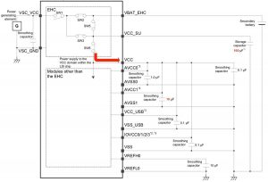 The design simplicity stems from the full set of functional blocks contained within the RE01 MCU as shown in Figure 4.
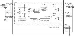 Along with its functional blocks, the EHC provides several voltage monitoring circuits as well as multiple status and control registers to orchestrate power delivery. For example, a power generating element status flag (ENOUT) indicates whether that element is generating current. Conversely, a charging target monitoring flag (CMPOUT) indicates whether charging voltage is being applied to the secondary battery or to the storage capacitor. Each of these features plays a role as the EHC proceeds through the operational states associated with startup, normal operations, and battery exhaustion (Figure 5).
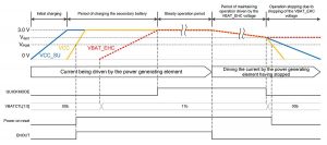 When a power generating element is connected to the MCU, the EHC enters the initial charging period. Here, the EHC enables power to flow to VCC_SU, charging the storage capacitor until the voltage level on VCC_SU exceeds a specific threshold voltage level, VCC_SU_H. At this point, the EHC then uses the storage capacitor to begin supplying power to the system domain, VCC. When VCC exceeds the power on threshold voltage (VPOR), the Power-on reset signal goes high, releasing the device from reset and simultaneously bringing ENOUT high, indicating that the power generating element is active.
After power on reset is released, the EHC’s VBAT_EHC charge control register, VBATCTL, is set to 11b, allowing the device to begin charging the secondary battery. In fact, during this period, the EHC alternates its charging output between the secondary battery and the storage capacitor to maintain the VCC supply while the battery is charging. When the storage capacitor voltage falls below a lower threshold voltage level, VCC_SU_L, the EHC switches power to VCC_SU until it reaches the upper threshold VCC_SU_H, at which point it resumes charging the secondary battery. This process continues until the storage battery voltage on VBAT_EHC reaches the VBAT threshold, VBAT_CHG (Figure 6).
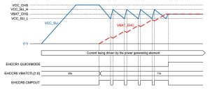 After the battery is charged, the QUICKMODE bit is set, causing the EHC to enter the steady operating state. In this state, the EHC continues to charge the battery from the power generating element, while simultaneously supplying power from the battery to the VCC domain.
If ambient energy falls and the power generating element stops providing power, the EHC continues supplying VCC from the battery. Eventually, the internal voltage monitor will detect that the VBAT_EHC has fallen below a preset threshold, Vdet1, and the QUICKMODE bit will be reset to zero. Once this bit is set, power is cut to the VCC domain and EHC registers are initialized. Further reduction in VCC below VPOR causes the device to reset the Power-on reset signal. To resume operation, the device must accordingly perform the initial charging sequence after ambient energy has risen to sufficient levels.
Evaluation kit aids rapid prototyping
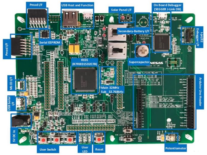
While the RE01’s built-in EHC eliminates the need for additional components, to utilize its features, developers still need to configure the device and execute the prescribed series of operations mentioned above. To help developers move quickly into rapid prototyping and custom development with the RE01 family, Renesas provides the RTK70E015DS00000BE and RTK70E0118S00000BJ ready-to-use evaluation kits for the RE01 1500KB and RE01 256KB, respectively. In fact, the RE01 1500KB kit offers a turnkey development platform that includes the RE01 1500KB MCU board (Figure 7), an LCD expansion board, a solar panel, and a USB cable. Along with the RE01 MCU, the development board includes a storage supercapacitor, a connector for an external rechargeable battery, switches, LEDs, an on-board debugger, and multiple interface connectors, including an Arduino Uno header.
Along with the hardware development platform provided in the evaluation kit, Renesas provides a comprehensive set of software packages designed to run under IAR Systems’ Embedded Workbench integrated development environment (IDE), or Renesas’ own e2 Studio IDE. Built on Arm’s Cortex Microcontroller Software Interface Standard (CMSIS) driver package, the software uses software constructs familiar to developers of code for Arm-based processors.
Perhaps most important, the sample routines in the Renesas software packages provide an executable template for custom software development. For example, implementation of the EHC operating sequence shown in Figure 5 requires an accompanying series of initialization procedures needed to minimize power consumption during key stages such as initial charging and secondary battery charging. A startup routine provided with the sample software demonstrates each of these initialization and setup procedures. Even better, Renesas provides developers with a clear path for using this startup routine to change parameters as needed and insert their own software code into the startup sequence (Figure 8).
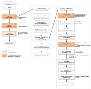 Using the Renesas evaluation kit and related software packages, developers can quickly explore different operating modes of the RE01 MCU and evaluate energy harvesting methods. Later, this environment provides an effective platform for rapidly prototyping their own application and custom development.
Conclusion
Energy harvesting offers an effective solution for reducing battery size and extending battery life in low-power systems like IoT devices, but the approach can add significantly to overall design size, complexity and cost. A more integrated approach is required.
Packed with multiple functional blocks and peripherals, a family of MCUs from Renesas includes a complete on-chip energy harvesting subsystem that streamlines and simplifies energy harvesting system design. Working with associated development boards and software, developers can quickly evaluate, prototype and build custom designs able to take full advantage of energy harvesting’s benefits using small, low-cost devices.


