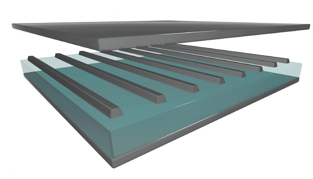
A Purdue University-led research team has simplified the manufacturing process that allows utilizing multiple colors at the same time on an electronic chip. By embedding silver metasurfaces, artificial materials thinner than light waves, inside optical cavities they drastically scaled down the thickness of the cavities and broadened the potential color bandwidth for electronics and nanophotonics.
Currently, each color frequency requires an optical cavity of a different thickness. By reducing the metasurface-based nanocavity thickness below the conventional minimum, the team, which also included researchers from Stanford University and the University of Maryland, was able to achieve a uniform thickness that could be used for all colors.
The team experimentally showed that nanostructured metasurfaces within 100-nm nanocavities could support resonances within the wavelength band from 500 to 800 nm. The researchers demonstrated successful application of the fabricated nanocavity samples as on-a-chip ultrathin color filters.
The cavity resonance can be tuned not only by adjusting the cavity thickness, but also by adjusting the parameters of the metasurface. In experiments, several cavities having the same thickness were implemented on the same planar chip. The researchers were able to obtain different resonant wavelengths by controlling the width of nanostructured metasurface elements. Multi-band filtering, coloration, and imaging were made possible inside the same cavity by controlling the degrees of freedom provided by the metasurface.
The ultrathin optical cavities could be used in integrated optical systems on-a-chip such as VCSELs, high-resolution spatial light modulators, imaging spectroscopy systems, and bio-sensors. “Our nanocavities would make on-a-chip lasers ultrathin and multicolor,” said Alexander Kildishev, associate professor of electrical and computer engineering at Purdue University.
Optical metasurfaces could also ultimately replace or complement traditional lenses in electronic devices, the researchers believe. “What defines the thickness of any cell phone is actually a complex and rather thick stack of lenses,” Kildishev said. “If we can just use a thin optical metasurface to focus light and produce images, then we wouldn’t need these lenses, or we could use a thinner stack.”


