By Charlie Osburn
Silicon cannot take our computing power as far as we would like, but researchers believe other materials can.
Researchers hope the future of our semiconductors lies not within silicon, but new materials which can be used to create transistors ten times smaller than our current circuitry.
Stanford Associate Professor of electrical engineering Eric Pop and post-doc Michal Mleczko revealed a new study into the applications of semiconductor material potentially able to support computer chips just a few atoms thick.
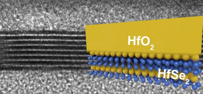
Published in the academic journal Science Advances, the engineers report how two semiconductors, hafnium diselenide, and zirconium diselenide, either share or go beyond the traits that make silicon such a popular semiconductor today.
All three, for example, can “rust.” While you would be forgiven for thinking that rust is not generally a desirable feature for metals and materials, in this case, the “rust” — encouraged by exposing silicon to oxygen during manufacturing — isolates and protects the circuitry.
The two new semiconductor materials do the same, which eradicates the need to add additional insulators, bringing up the cost and time to produce computer components. However, hafnium diselenide and zirconium diselenide are “high-K” insulators, which require less power to operate than silicon and silicon oxide insulators.
Pop and Mleczko say that the materials outperform silicon further as they can also be shrunk to functional circuits just three atoms thick. Sadly for silicon, five nanometers is usually the limit without causing breakages or leaks, and these materials can be modified to be ten times smaller.
“Engineers have been unable to make silicon transistors thinner than about five nanometers before the material properties begin to change in undesirable ways,” Pop said.
While other semiconductor materials also beat silicon in these categories, the problem is often that the energy required to switch transistors on, the “band gap,” causes material circuits to leak, become unreliable, or break outright. However, hafnium diselenide and zirconium diselenide are considered “just right” in the same manner as silicon as they work in what is considered the optimal range which keeps chips energy-efficient and reliable.

Michal Mleczko
Although still experimental, the researchers say the materials could become a bedrock for thinner, more energy-efficient chips in the future.
“Silicon won’t go away,” Pop said. “But for consumers, this could mean much longer battery life and much more complex functionality if these semiconductors can be integrated with silicon.”
The researchers warn there is a long road ahead before we can expect ultrathin semiconductors as essential components in new computer systems. Mleczko and Pop’s next task is to refine and improve the electrical contact between transistors on their diselenide circuits, a process which becomes more difficult the thinner the circuit becomes.
When working on the atomic scale, this is not expected to be a quick project.
In addition, the team must learn how to better control oxidized insulators to become as thin and stable as possible.
Once this research is complete, the components will then be integrated and scaled up to working wafers, complex circuits, and then — hopefully — fully operational systems.
“There’s more research to do, but a new path to thinner, smaller circuits — and more energy-efficient electronics — is within reach,” Pop says.
The research was supported by the Air Force Office of Scientific Research (AFOSR), the National Science Foundation, Stanford Initiative for Novel Materials and Processes (INMP), the Department of Energy (DOE) Office of Basic Energy Sciences, Division of Material Sciences, and an NSERC PGS-D fellowship.
Article Courtesy: www.zdnet.com
Author: Charlie Osborne is a cybersecurity journalist and photographer who writes for ZDNet and CNET from London.


