By: Harmeet Singh
- Lam Research has been an etch leader for decades, including by pioneering technology in cryo etch
- The age of AI demands breakthrough innovations in memory architecture, especially in NAND
As we stand on the brink of a new era in technology, marked by the rise of artificial intelligence (AI), the demand for more advanced computational capabilities is skyrocketing. Data-intensive AI applications require significant advancements in memory technology—particularly in NAND flash memory, including faster data transfer speeds.
A side effect in the surge in compute demand is an increase in power consumption to handle data transfers within memory systems. In other words, the escalation contributes to heightened energy use in data centers because compute for AI training consumes a significant amount of energy (and space on the chip). Deploying high-density and more power-efficient NAND storage, which is used in more energy-efficient solid-state drives (SSDs), addresses the performance, space, and power requirements while reducing the operating costs and environmental impact of the AI revolution.
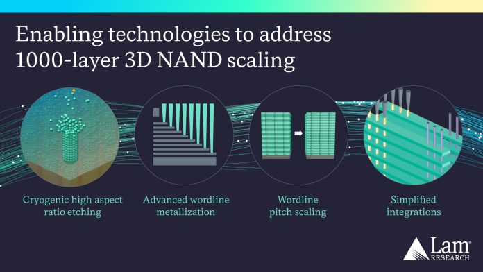
At Lam Research, we are at the forefront of driving these innovations, including those needed to scale 3D NAND to 1,000 layers by the end of the decade.
The path to 1,000-layer 3D NAND is more than a visionary milestone—it’s a necessity driven by the burgeoning demands of AI and machine learning technologies. These applications rely heavily on vast amounts of data to train algorithms and process information efficiently and effectively.
3D NAND chips with 1,000 layers will boost data storage capacity and throughput—crucial for AI applications that require rapid data retrieval and processing. As such, the semiconductor industry is pushing physics and chemistry to their limits, striving for higher data storage capacities and faster processing speeds.
Unfathomable Complexity
3D NAND flash is a type of memory that stacks multiple layers of cells vertically, increasing the density and capacity of data storage. The architecture involves complex and precise processes that require breakthrough innovations in etch and deposition technologies.
Etching is the process of removing material from the surface of a wafer to create the desired patterns and structures for memory cells. Etching is a critical process step to enhance 3D NAND device performance, reliability, and yield.
Scaling 3D NAND to higher layer counts is no trivial task. We’re talking about manufacturing at an atomic scale—1,000x smaller than the width of a human hair. The technologies and processes that got us from 2D to 3D, and from 64- to 232-layer 3D NAND are not capable of getting us to 1,000 layers without new breakthroughs. That’s why we must continue to innovate our precision high aspect ratio etch capability to enable our customer’s roadmap.
“Memory hole precision” refers to the accuracy in creating vertical pathways in the memory stack that connect the cells, which is crucial for scaling 3D NAND devices to higher layer counts without compromising quality. “Logic scaling” requires reducing the deviation in critical dimensions from the top to the bottom of the channels, which is essential for the performance and capacity of flash memory as it scales to more layers and correspondingly taller stacks. The goal is to maintain the critical dimensions of the channels from top to bottom without deviation, which is essential for the performance and capacity of flash memory as it scales to more layers.
Just because you can technically scale the number of layers doesn’t mean you can move to high-volume production. To scale, flash manufacturers must increase performance and capacity while decreasing the cost per bit.
The combined operational and technical complexity approaches the unfathomable.
Trend Setter
At Lam Research, we don’t follow trends—we set them. Lam’s pioneering efforts in etch and deposition technology over the decades have led to significant breakthroughs in NAND flash manufacturing. We have a proven track record of delivering solutions that enable 3D NAND scaling, such as cryogenic memory hole etch, which is the process of creating vertical pathways in the memory stack that connect the cells. This process is essential for enabling 3D NAND devices to scale to higher layer counts, as it determines the quality and uniformity of the memory cells.
Lam has improved memory hole etching processes over time, using our unique and proprietary technologies, such as:
- Cryogenic high aspect ratio etching with novel chemistries, a uniform deep etch that lowers wafer temperature during manufacturing to enable innovative new process chemistries that allows for more bits per cell.
- Scalable high-power confined plasma reactors, which generate high-energy plasmas that can etch deep and narrow holes with high aspect ratios.
- Unique pulsed plasma technology, which modulates plasma species to control the etch profile and selectivity, resulting in more uniform and consistent holes.
With these technologies, Lam has enabled our customers to achieve near-perfect memory hole etch profiles with high throughput and, because of greater efficiency, low environmental impact.
NAND Scaling
Lam has also enabled our customers to scale 3D NAND laterally, vertically, and logically with our leadership in high aspect ratio (HAR) etch. A differentiated high aspect ratio etch capability enables our customers to scale multiple vectors:
- Lateral scaling, which involves reducing the dimensions of individual memory cells and the distances between them in the same area, increasing the bit density and capacity.
- Vertical scaling, which involves increasing the number of layers in the memory stack to achieve higher storage capacity, performance, and energy efficiency.
- Logic scaling, which means increasing the number of bits per storage cell—from single-level cell (SLC) to multi-level cell (MLC), triple-level cell (TLC), and even quad-level cell (QLC)—allowing for more data to be stored in the same physical space.
Lam’s high aspect ratio etch solutions, such as Flex and Vantex, use advanced hardware and software technologies to deliver precise dielectric etching with exceptional uniformity, repeatability, and low defectivity to create the most critical HAR device features.
In sum, our solutions enable our customers to reduce costs by packing more cells per layer, which increases the number of layers, and get more bits per cell, thereby improving energy efficiency and optimizing performance and reliability—necessary features that enable the AI era.
Defining Tomorrow
As we navigate the complexities of the AI age, the path to 1,000-layer 3D NAND represents more than just a technological aspiration; it symbolizes a leap toward meeting the future demands of global data processing and storage. Lam Research is committed to leading this charge, providing solutions that address the critical challenges of today and paving the way for innovations that will define tomorrow.


