Applications such as power factor correction (PFC) in computer servers and telecoms systems or hard-switching PWM stages in UPS and solar inverter designs demand ever-increasing power outputs without corresponding increases in space. The imperative to improve power density means that designers must find ways to meet high-speed performance criteria while driving up efficiency and minimising heat.
In the case of power switching devices such as MOSFETs, thermal limitations have represented a significant barrier to migrating away from traditional leaded MOSFETs to surface mount alternatives. Now, however, a combination of improved super junction (SJ) semiconductor processes and advances in SMD package design is enabling the first SMD MOSFET technologies compatible with the requirements of today’s medium- to higher-power schemes.
We live in a data-hungry age where power and real estate costs are rising. These two facts have a huge impact on much of the infrastructure that forms the backbone of our connected world. And with the expectation that every new generation of technology delivers more power than the previous in a smaller footprint – the impact on power density is enormous.
Modern servers, for example, demand increased power at lower voltages. This brings challenges as currents rise rapidly requiring more and more copper to transmit the power efficiently. Looking at today’s data centers, it is no surprise that power densities per rack are rising – space is at a premium and businesses are trying to wring more profit from every square foot. Back in 2006 there was around 6 kW in each rack – by the end of this decade that is predicted to have almost trebled – putting ever-increasing pressure on power system designers.
Clearly, efficiency plays a large part in addressing this challenge. One of the truisms of power is that ‘you don’t have to deal with heat that you don’t generate’. High efficiency means that more useful power is transmitted to the task in hand – computing, telecoms or solar – saving energy costs. It also allows for a greater density of servers, which reduces real estate costs. But that’s not all; as less waste heat is generated, the cooling requirements also reduce, which again saves space and reduces energy costs.
The journey to design a highly efficient, extremely dense power system begins with the topology chosen and, in particular, the performance of the main power components. That’s why semiconductor companies continue to refine their processes and develop new technologies that improve the key ‘Figures-of-Merit’ (FoM), which leads to greater efficiency. But, that is only half the story. While the world moved to surface mount devices years ago, power switches have lagged behind; many of the ‘latest semiconductor advances’ are still housed in pin-in-hole packages (TO-220 and TO-247 being the most popular). Such packages may bring benefits to thermal management but they often necessitate a second production process that drives cost. In addition, the package leads themselves can be a barrier to performance, as we shall see.
C7 Gold Super junction Process
Infineon Technologies’ CoolMOSTM process is a proven technology that has benefitted from substantial development since the introduction of its novel drain structure back in 1999. The process also supports the highest quality standards, as illustrated by the fact that from the last 1.6 billion CoolMOSTM units shipped there have only been 38 failures.
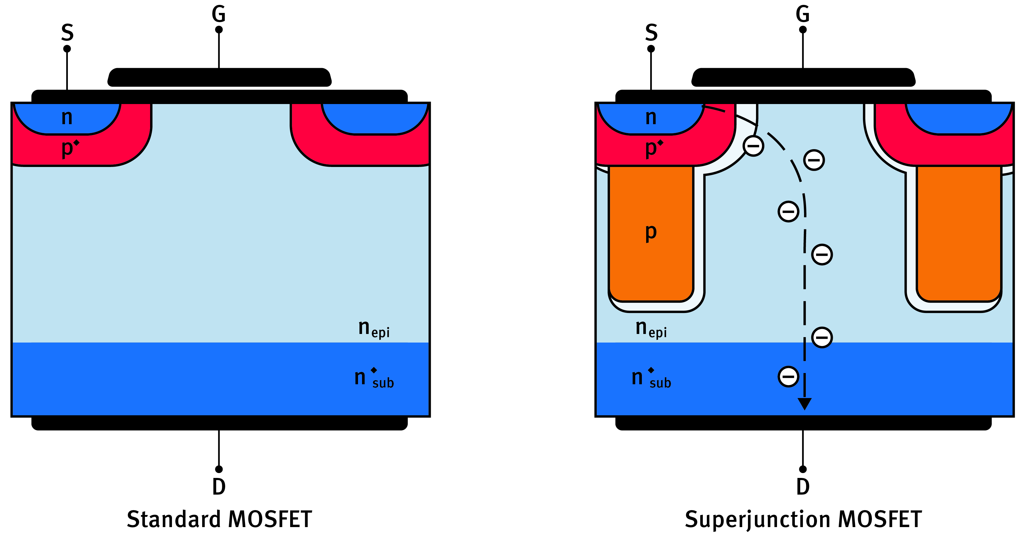
Figure 1: Comparing the structure of a Super junction MOSFET to a standard MOSFET
There are two key principles employed in super junction CoolMOSTM MOSFETs. First, the on-state resistance (RDS (ON)) is lower as the main current path is much more heavily doped than for a conventional high-voltage MOSFET. Without the p-columns forming a charge compensation structure below the cell structure the transistor would have a much lower blocking voltage capability due to the highly doped n-region. The precisely sized and doped p-columns constitute a “compensation structure”, which balances the heavily doped current path and supports a space charge region with zero net charge supporting high blocking voltage.
This construction enables a reduction in area specific resistance that improves conduction loss. The attendant reduction in chip area was remarkable and CoolMOSTM technology reduced capacitance and dynamic losses, which allowed the silicon limit line to be beaten. The first generation, CoolMOSTM CP further improved all aspects of losses.
This MOSFET technology approach has been continually developed – the C7 generation continued to reduce capacitances and achieved an R (ON)*A below 1 Ω*mm2 for the first time. The turn-off losses in C7 were 50 percent less than the earlier CP generation. C7 Gold (G7) takes this well-established manufacturing technology further, reducing turn-off losses by a further 25 percent and ensuring ‘best-in-class’ FoM in terms of both RDS (ON)*EOSS’ and RDS (ON)*Qg. This leads to higher system efficiency in hard-switching topologies, such as Power Factor Correction (PFC).
TO-Leadless (TOLL) packaging
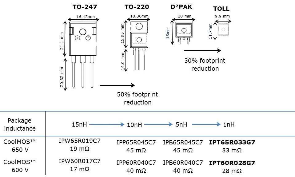
In many mid-to-high power PFC circuits it is not uncommon to see pin-in-hole packages in the power stage. As electronics has improved, package engineering has also seen innovation (TO-247 became TO-220 offering a 50 percent footprint reduction) yet, even the surface mount D2PAK had pins (albeit surface mountable).
The issue with pins is not just that pin-in-hole technologies require a different manufacturing process such as wave reflow or, worse still, hand soldering – pins introduce inductance into the package. This parasitic inductance counteracts the drive voltage and the ensuing slower transient reduces efficiency.
This is where the new TO-Leadless (TOLL) package from Infineon comes in. Figure 2 shows this package in comparison to previous form factors.
Figure 2: Comparing Infineon C7 and G7 technology, package sizes and inductances plus RDS (ON) max values
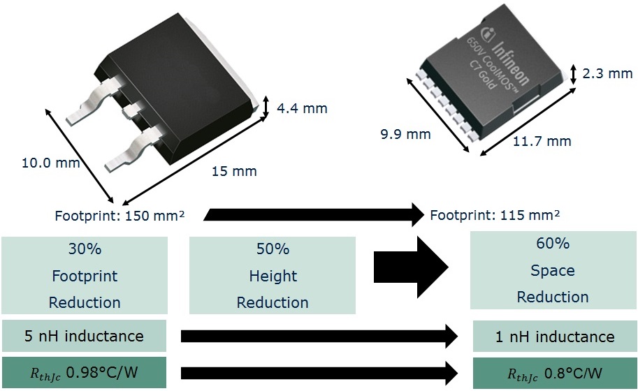
Figure 3 compares more closely the TOLL package with a traditional SMD package such as D²PAK. Not only does the new package eliminate the leads associated with pin-in-hole technology and, consequently, reduce the package inductance from 5 nH to 1 nH but it also offers an impressive 60 percent reduction in space used.
Figure 3: TO-Leadless (TOLL) shows significant size and performance benefits over D2PAK
The new TOLL package brings benefits in manufacturing; the totally Pb-free package has an MSL1 rating for easy handling on the shop floor and is compatible with both wave and reflow soldering, offering high levels of flexibility. Moreover, the tin-plated leads feature a trapezoidal groove next to the PCB pad. This guarantees wetting and means that the joint is fully visible for optical inspection systems, ensuring the quality of the finished product.
600V and 650V V CoolMOSTM C7 Gold MOSFET in TOLL package
Bringing together the benefits of the CoolMOSTM C7 GOLD (G7) process and the advantages of a TOLL package for the very first time, the IPT65R033G7 and the IPT60R028G7 are a new type of power transistor that offer engineers some significant benefits when it comes to next-generation power designs.
The package can be connected in a standard 3-pin MOSFET configuration or with the option of an additional connection to the source (Kelvin connection). This can be used as a reference potential for the gate drive voltage, thus eliminating voltage drops due to the (much reduced) 1 nH parasitic inductance in the source pin. This crucial feature enables easy, higher efficiency operation – particularly in full load conditions.
The IPT65R033G7 and the IPT60R028G7 offer the industry’s lowest on resistance of just 33 respectively 28 mΩ (max). This coupled with a typical gate charge (Qg) of just 110 nC and an Eoss of 13.5 uJ at 400 V for the 650V device ensures that the key FoM for these devices are truly best-in-class.
Housed in the new TOLL packaging, the IPT65R033G7 and IPT60R028G7 measure only 10.10 mm x 11.88 mm x 2.4 mm. The lead-free approach to die attach is responsible for a typical thermal resistance from junction to ambient (RthJA) of just 35 °C/W in the SMD device. Such thermal properties allow an SMD power device to be used in hard-switching PFC circuits up to 3 kW for the first time. While the use of the 650V C7 Gold (G7) technology is limited to hard switching topologies the 600V version comes with the additional feature of a robust body making it suitable also for resonant switching applications such as LLC.
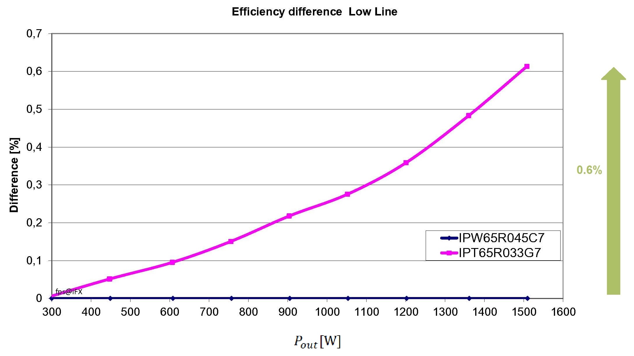
The new C7 Gold (G7) technology delivers real performance benefits that have a material impact on state-of-the-art power designs as can be seen in the following performance charts.
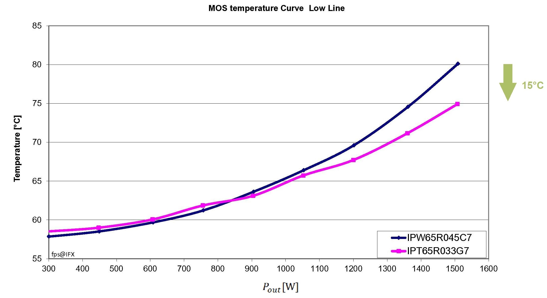
Figure 4: The higher efficiency from TOLL package Vs the much larger and traditional TO-247 package is due to lower RDS (ON) and use of the 4-pin Kelvin Source connectionFigure 5: Lower temperature is due to the higher efficiency generated by the C7 Gold technology and the use of the 4-pin Kelvin Source connection
Summary
The key benefits of C7 Gold technology of low Ron*A (<1 Ω.mm²) enables low RDS (ON) (33 mΩ for 650V, 28 mΩ for 600V) to be achieved. Improved FOM such as RDS (ON)*EOSS and RDS (ON)*Qg together lead to efficiency improvements and the generation of less thermals.
Efficiency is then enhanced further with the TOLL package features of low package source inductance (~1nH) and the use of the Kelvin Source 4th pin option.
Combined with the small footprint (115 mm²) and improved thermal performance of the TOLL package (RthJA of 35 °C/W) , this leads to a MOSFET technology that enables designers, for the first time, to use an SMD package in switched mode power supplies up to 3 kW.
This aligns directly with the requirements for modern server, telecom and solar power supplies in the continued push for higher power density and cost reduction through automated production processes.
The high quality of the TOLL package with its MSL1 rating and compatibility with both reflow and wave soldering techniques brings benefits in manufacturing these long lifetime applications. The package is also qualified for industrial applications according to JEDEC (J-STD20 and JESD22) and will soon migrate to house other technologies such as Infineon’s CoolGaN product portfolio.
Dr. Stefan Gamerith, Infineon Technologies AG
With a Phd in physics Stefan Gamerith joined Infineon in 2007. After several years as a project manager for different CoolMOS™ Technology development projects he changed to a product marketing position in 2015. Since March 2017 he is leading the PMM ACDC HVC high power product marketing group.
ELE Times provides a comprehensive global coverage of Electronics, Technology and the Market. In addition to providing in depth articles, ELE Times attracts the industry’s largest, qualified and highly engaged audiences, who appreciate our timely, relevant content and popular formats. ELE Times helps you build awareness, drive traffic, communicate your offerings to right audience, generate leads and sell your products better.


