Our cellular networks must provide cost-effective, reliable and secure timing. Therefore, the infrastructure requires proper architecture, design and management. Part two of this discussion continues our examination of 5G networks and performance.
Introduction to Timing Requirements and Design Techniques Used to Synchronize 5G Networks
5G networks rely on time division duplex (TDD) networks that require accurate phase and time synchronization to ensure fast and reliable operation. To deliver accurate frequency, phase and time across the 5G network, the equipment utilized in TDD networks use a combination of Global Navigation Satellite System (GNSS), Synchronous Ethernet (SyncE) and the IEEE-1588 Precision Time Protocol (PTP).
In this two-part blog post, we will review the timing requirements and design techniques used to synchronize 5G networks. In part one, we covered the new 5G Radio Access Network (RAN) architecture, timing standards and basic time-accuracy requirements. Here, we will discuss the architecture and techniques needed to meet the critical requirements for 5G timing design.
Design for Timing

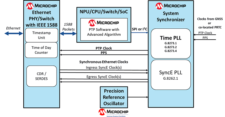
Figure 1 depicts a standard block diagram of the major components used to maintain, control and deliver timing in equipment design. It can be used as a guide when developing Centralized Unit (CU), Distributed Unit (DU) or Radio Unit (RU) applications.
The main element in the timing design is a system synchronizer consisting of one or more sophisticated phase-locked loops (PLL) offering the functionality required to give precise frequency and time synchronization. Synchronizers, like the ZL3073x family of advanced PLLs, control clock monitoring, reference switching, filtering and syntonizing accurate clocks that keep equipment synchronized to network time. Numerous PLLs within the same synchronizer enable support of SyncE, PTP and additional time requirements. Synchronizers supporting several inputs and outputs can monitor and syntonize clocks for a variety of interfaces. The Time PLL (figure 1) can also be restricted to pulse per second (PPS) inputs from local Primary Reference Time Clocks (PRTCs) or other equipment that provide PPS references. The PLLs designed into the ZL3073x devices support a fast lock to 1Hz, or PPS, mode that greatly improves the time it takes to lock to external PPS references. This reduces the lock time for equipment connected to external PPS references down to seconds instead of minutes.
For SyncE support, one or more recovered clocks link to the system synchronizer, which will certify and oversee the various input references. The synchronizer chooses one recovered clock as the primary clock; the SyncE PLL will filter the clock before allocating it to the egress nodes again. If support is required for the eEEC, as defined in G.8262.1, it is essential to guarantee that the SyncE recovered clock can be swiftly squelched on a Loss of Signal (LOS) condition. This verifies that the short-term and long-term phase transient limits of G.8262.1 can be fulfilled.
Correct implementation of PTP involves accurate timestamping capabilities and dedicated software to appropriately provide precise time synchronization. Timestamp units must be located as close to the edge of the box as possible to minimize delay. A timestamp unit with 10 nsec of accuracy is acceptable for Class B equipment. To satisfy Class C clock constraints, timestamp units may need to have an accuracy of 4 nsec or better. A PTP software stack and a robust time algorithm—most vital—is required to manage PTP packet communication, process timestamps and make frequency and phase modifications to the Time PLL inside of the system synchronizer. For over 15 years, we have developed and maintained our own PTP stack that ensure network interoperability. Additionally, our advanced algorithm provides market leading performance for a wide range of deployments and network traffic conditions.
Our portfolio of Ethernet PHYs consists of a variety of solutions capable of meeting the timestamping requirements outlined above. The META-DX family support rates from 1 GbE to 800 GbE with high-accuracy timestamping and constant latency to help optimize for 5G designs. Our line of copper 1G PHYs (VSC8574, VSC8584) and 1/10G optical PHYs (VSC8584, VSC8490, VSC8258) also support high-accuracy timestamping with accuracies down to +/- 2ns. Additionally, these dual and quad PHYs offer MACsec encryption/decryption without impacting the accuracy of the PTP traffic.
Finally, a precision oscillator offers the frequency base at startup and guarantees stable operation in cases of network disruption. Not all use cases will demand robust holdover abilities, but as the equipment is positioned further into the core of the network, the oscillator must be increasingly stable. The caliber of the local oscillator, the operating environment (temperature, pressure, and voltage), and the duration of the network disruption are just some of the key factors that need to be considered when determining the holdover performance needed for your system. Depending on these factors, higher end Oven-Controlled Crystal Oscillators (OCXOs) or lower cost Temperature Compensated Crystal Oscillators (TCXOs) may be suitable for some use cases. We offer a variety of oscillators capable of meeting the most stringent requirements as well as lower cost solutions offering simpler holdover performance. For more information on oscillator selection for SyncE and IEEE-1588 applications please refer to our application note AN3467.
Class C and Class D Design Considerations
Be mindful when constructing the timing architecture in systems required to comply with the class C and D requirements. You can utilize calibration techniques to correctly manage the constant time error (cTE) and dynamic time error dTE within a given design in addition to enhanced timestamp accuracy and the need of providing squelching capability for the ingress eEEC on LOS conditions. As engineers work to decrease the time error that equipment presents, accounting for on-board or in-system calibration has become more common and essential. At the time of component selection, identifying potential sources of cTE due to process, temperature and voltage needs to be taken into consideration.
You need to lessen delays created by buffers, FPGAs, timestamp units or other devices in the timing path and, if you can, fix them with calibration techniques at the board and/or system level. Input-to-output propagation delays through buffers and other devices can be allotted for by offering a feedback path back to system synchronizers that enable dynamic calibration of delay. Due to the relative time-error requirement created by the advanced time accuracy constraints, it is no longer enough to only focus on the input-to-output delay of a box; you also should take notice of the output-to-output alignment for each PPS output within a system. Moreover, for chassis equipment, the line card PLL bandwidths for each output should be the same or programmed as high as possible to certify that the equipment manages any phase changes as identically as possible across all outputs.
Synchronizers, like the ZL30735, timestamping PHYs and switches can offset known delays which are inherent in board designs. From a board level, static calibration techniques can make up for trace delay and propagation delays on a per-output or per-port basis. Synchronizers can deliver per-input trace delay and buffer compensation, picosecond phase adjustment resolution, per output trace delay compensation and per-input or per-output cable delay compensation for GNSS or G.703 1PPS interfaces. In addition, advanced timestamping devices offer per-port timestamp calibration with picosecond resolution. These features offer flexibility to measure and adjust for phase error within a system to guarantee TE is decreased.
Our Timing Heritage and Solutions
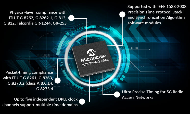
As the market leader in network synchronization, our latest products offer the features and performance to simplify board design and help to satisfy the stringent time requirements needed for 5G systems. The ZL30735 family of network synchronization PLLs offer up to five independent clock channels with support for up to 10 inputs and 20 outputs. Our PLLs provide the clock monitoring, reference switching and holdover features needed. In addition, we have designed these devices to minimize phase error due to input-to-output delay and delay variation between outputs. To aid in calibration of more complex designs, our PLLs offer measurement and compensation features that allow you to minimize trace and propagation delay throughout your system.
Finally, our PTP stack and advanced algorithm software provide a comprehensive solution for your network synchronization needs. This software can run on a variety of host processor architectures, whether embedded into an SoC (such as our PolarFire® SoC FPGAs) or on a dedicated CPU. Additionally, the software packages are maintained to be backwards compatible to our previous generation PLLs as well as continuously upgraded to support new standards and network deployment scenarios that arise.
To support the ultra-low latency, high bandwidth and advanced new radio applications for 5G and beyond, synchronization requirements and capabilities continue to evolve. Meeting the new enhanced standards for time accuracy in network equipment demands careful planning of the timing architecture. Our leading-edge network synchronization PLLs and software will help assist you in meeting these advanced synchronization requirements. Check out our web page to learn more about 5G timing. For more information about 5G network infrastructure and GNSS and ePRTC 5G timing architectures, visit our web pages.


