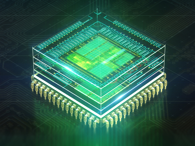
Transitioning from 2D to 3D IC architectures is not as simple as creating multiple systems-on-chips (SoCs) and blindly stacking them together. There is a lot of tools required and methodologies impacting the 3D IC architecture. When it comes to generating the highest performance at the lowest achievable power, 3D architectures are by far the more optimal solution. 3DICs are naturally suited to support compute-intensive workloads by allowing extreme, heterogeneous, and homogeneous integration that provides for the densification and scalability that 2D architectures lack.
Out ELE Times correspondent and Sub Editor Sheeba Chauhan took this opportunity to interact with Rituparna Mandal, General Manager, MediaTek. The conversation was indeed very insightful and informative.
Excerpt:

ELE Times: How are 3D ICs impacting networks, graphics, AI/ML and high-performance computing?
Rituparna Mandal, General Manager, MediaTek – Semiconductor makers have been suffering from a lack of space to build additional capacity and, with the introduction of 3-dimensional integrated circuits, this issue is being resolved. They act as a natural option for applications keen on creating advanced use cases. 3D ICs are greatly impacting networks, graphics, artificial intelligence, machine learning and high-performance computing, given their innovative capacity for vertical stacking. Through this method, 3D ICs offer faster inter-connections between the applications while possessing a smaller footprint compared to multiple packaged chips. 3D ICs also offer better yield than single dice, while ensuring flexibility and allowing the intermingling of different manufacturing processes. Further, the possibility of reusing existing chips, without redesigning the entire structure, makes 3D ICs all the more beneficial and ideal for new age technologies.
ELE Times: What can be the alternative to the single-die SoC approach to place multiple bare dice into a single package?
Rituparna Mandal, General Manager, MediaTek – One of the major factors bolstering the semiconductor industry is the fact that it is based on innovation. Therefore, the industry has managed to successfully double the number of transistors in a silicon chip consistently, over the years. This has led to the creation of an array of innovative semiconductor products and solutions. 3D ICs have acted as a suitable alternative to single-die SOCs, enabling the possibility of placing multiple dice into a single package. In fact, the new age monolithic 3D SoCs continue building on multiple active silicon layers while placing vertical interconnects between these layers, creating a highly power packed option for SOCs. This method has ensured that smartphones today can crunch data as humungous as the ones crunched by gigantic servers in yesteryears.
ELE Times: What strangleholds do you see in POP (Package-on-Package) packaging? Can it be categorized as 3D packaging?
Rituparna Mandal, General Manager, MediaTek – Packaging is a huge part of the semiconductor creation process for it acts as protection against physical damage and corrosion. During the final leg of the manufacturing process, these packages protect everything from silicon wafers, and logic units, to the chip’s memory. Given that different ICs require disparate packaging requirements, the semiconductor packaging segment has huge opportunity for growth and meeting the challenges.
ELE Times: What are the advantages of 3D IC over traditional SOC (system-on-chip)?
Rituparna Mandal, General Manager, MediaTek – 3D ICs have a variety of advantages when compared with traditional SOCs. They are ideal for applications which require more transistors in a specific footprint. Take mobile chips for instance – these use cases require transistor densification, but their capabilities are limited by footprint and height constraints. In such scenarios, 3D ICs act as superb alternatives. It also ensures the creation of highest-margin, highest-volume designs. With the demand for bandwidth doubling every few years, 3D ICs can offer a sustainable way forward for the semiconductor market.
ELE Times: What extraction and analysis tools are crucial for designing 3D ICs?
Rituparna Mandal, General Manager, MediaTek – Design convergence on 3D ICs require a variety of extraction and analysis tools and, with the technology gaining popularity, these tools need to be extended for 3D IC use cases. The new tools, which are crucial to this set-up, must take into account issues such as layout parasitics for TSVs, micro-bumps, and interposer routing. The tools also need to be 3D-aware and innovative to meet the requirements.
ELE Times: Cost-effective 3D-IC design requires the co-design of three domains—chip, package, and board. What could be the other elements that can make 3D ICs most cost effective?
Rituparna Mandal, General Manager, MediaTek – Indeed, the co-design of chip, package and board are the most important requirements for cost-effective 3D IC design. In addition, the fact remains that cost-effective designs cannot be created by merely adhering to previously used techniques. While the three-way optimization technique for power, performance and area is still relevant, designing must also take optimization per cubic millimeter into account, as against the previously used metric of per square millimeter. In 3D ICs, designers must always keep the vertical dimension in mind. Designers should co-design the silicon IP, chiplets and package together for the best and most cost-effective outcomes.
ELE Times: What could be the major challenges in testing a 3D IC?
Rituparna Mandal, General Manager, MediaTek – Since 3D IC is still a new and unexplored field, test techniques and solutions are not yet fully evolved. Research is underway, and the segment is consistently striving towards creating better test cases. One of the biggest challenges is the fact that there is still so much that is unknown. Experts are working on the solutions and have already identified challenges related to the lack of probe access for wafers, thermal issues, proper access to stacked wafer modules, testability of the created designs, the economic concerns, etc. The possibility of defective designs is another challenge being faced in the vertical of testing 3d ICs.
Sheeba Chauhan | Sub Editor | ELE Times


