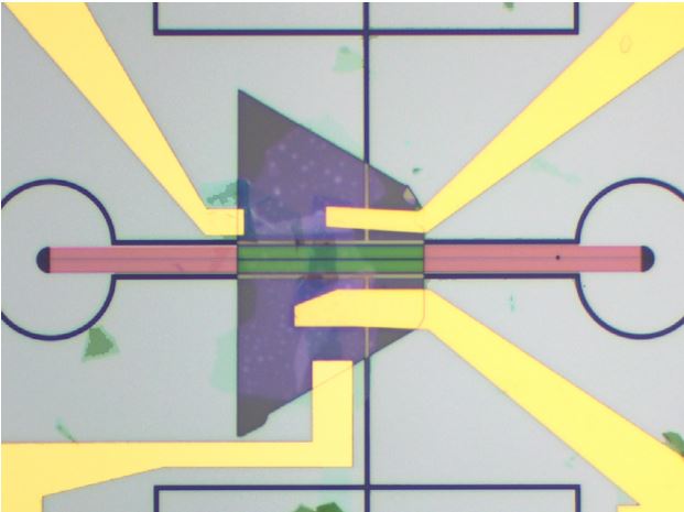
Researchers at MIT have developed a fabrication method for integrating silicon photonics with layered two-dimensional material molybdenum ditelluride (MoTe2) to create a single device that acts as both a light-emitting diode and a photodetector.
This work could have a dramatic impact on the field of silicon photonics, which has become a leading architecture in chip-integrated optical interconnects. This popularity stems, in part, from the promise that many components, such as waveguides, couplers, interferometers and modulators, could someday be directly integrated on silicon-based processors.
This latest MIT research could smooth the path to this level of integration because it represents the first time that an electrically powered light source enabled by a 2D material has been integrated on a passive silicon photonic crystal waveguide, according to the researchers.
Compared with traditional light sources such as III-V semiconductor lasers, which are usually wafer-bonded on the photonic circuits, the integration of MoTe2 with silicon would yield devices with much smaller footprints. It also raises the possibility that multiple low-power, direct-modulated light sources distributed in one place can be more advantageous than one, or a few, high-power lasers distributed across many transmitter modulators for use in high-performance computing systems.
While other 2D materials such as molybdenum disulfide and tungsten diselenide have been used in combination with silicon in this way, this work represents the first time a light emitting diode based on monolayer or bilayer MoTe2 has been realized.
This departure from other 2D materials is significant because, unlike these other materials, the emission wavelength from MoTe2 falls outside of the silicon absorption range. This leads to silicon absorption loss is dramatically reduced.
All of these 2D materials belong to a class of materials known as transition metal dichacogenides (TMDs). When these materials are taken from their bulk state down to two dimensions, they acquire interesting new properties. Among them is going from having an indirect band gap to a direct one.
In the case of molybdenum ditelluride, that direct bandgap is near ~1 eV. This means that the light-matter interaction in the 2D material is very strong and the material itself is a good candidate for light-emission and photon-detection.
Because of the small electron density states in a 2D material, it is possible to use electrostatic gates to control the electron or hole doping level in the material. In research described in the journal Nature Nanotechnology, the MIT researchers fabricated two separate metal gates to exploit this new capability.
“We created a monolayer (or bilayer) MoTe2 p-n junction where the electrons and holes can combine to emit light or be separated to form current, as the p-n junction works as either an LED or a photodetector,” said Yaqing Bie, a postdoctoral associate at MIT and co-author of the paper.
In the last step, Bie and his colleagues paired the bilayer MoTe2 p-n junction and a silicon photonic crystal waveguide. In this way, the light emitted from the LED can go through the waveguide to another place, and the p-n junction can detect the light coming from the waveguide as well.
The combination of 2D layers and the silicon substrate is smaller than photonic devices based on traditional wafer-bonded III-V lasers. What’s more, these 2D light source and detector units could potentially improve the communication speed of photonic devices.
While Bie concedes that a few more steps have to be undertaken by engineers before this technique could be used commercially, its potential in commercial applications is attractive.
One area that appears promising is high-speed data communication. In this case, by combining the light source with efficient on-chip modulators, it would become possible to further increase the optical coupling efficiency, which is the efficiency of optical power transfer between two optical components. It would also allow for wavelength division multiplexing, in which light signals are sent at many separate wavelengths through the same glass fiber.
Bie added: “We are trying to improve the light source efficiency and coupling efficiency by integrating with nanocavities. Integrated circuits with emitters, modulators, waveguide, and detectors are also one of the plans in the near future.”


