Power conversion is essential for electronic products, from battery-powered Internet of Things (IoT) sensors to high-power solar inverters. In addition, increasing the use of renewable energy and broader adoption of electric vehicles depends on efficient and robust power conversion. This article looks at some of these developing trends and discusses the engineering challenges they present. It shows how some of these have been solved by the efficiency and size advantages of wide bandgap silicon carbide (SiC) technology in high-power applications. It also discusses engineering challenges and high-level architecture for a fast DC EV charger, comparing the discrete approach to an alternative approach which uses the F1 half-bridge module from onsemi
Design Challenges in High-Power Conversion
Power conversion changes one voltage level to another (higher to lower and vice versa). For example, the microcontroller in an IoT sensor typically runs off a 3.3V or 5V voltage rail. However, battery voltages are nominally 3.7V, meaning voltage conversion is necessary for the microcontroller to use. Similarly, voltage conversion is also required in higher power applications like solar chargers, uninterruptable power supplies, and electric vehicle chargers. Despite the significant difference in power levels between these applications, efficiency in the conversion process is crucial for them both. Inefficient power conversion results in energy dissipating as heat that can negatively impact the performance of the electronic circuitry itself. Removing this heat is a thermal design challenge.
Wide Bandgap Silicon Carbide Semiconductor Technology
The properties of the power semiconductor largely determine the efficiency of the power conversion process and how much heat is dissipated. While only in the order of milliohms (mΩ), conduction resistance, RDS(on), becomes a significant factor for high-power applications switching hundreds or even thousands of amps. Silicon-based (Si) semiconductor technologies have been pushed to the limit of their thermal and electronic performance, and newer semiconductor process technologies have been developed to replace them in power applications.
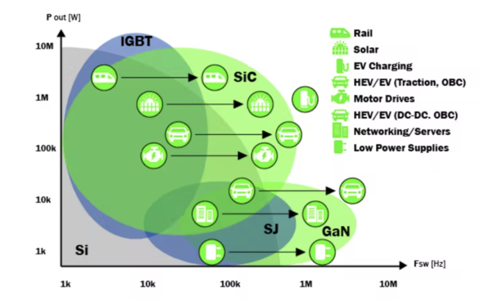
Wide bandgap semiconductors, like silicon carbide (SiC), have better thermal and electrical properties than silicon, allowing them to operate at faster-switching frequencies, higher voltages, and hotter temperatures. Figure 1 compares semiconductor technologies’ power handling and switching frequency characteristics in various end applications.
Figure 1: The power, switching frequency, and application use cases of different semiconductor materials (source onsemi)
SiC has many advantages compared to silicon, including thermal conductivity and an energy bandgap three times higher. SiC can operate at up to 1,200V compared to 600V with silicon, making it ideal for high-power power conversion applications like EV chargers. It also provides much better power density in smaller designs, a vital requirement feature for space-constrained EV chargers. As SiC process technologies have matured, costs have fallen, making it an even more attractive design option.
EV Fast Charger Architecture
The availability of fast-charging infrastructure will be critical for the broader adoption of electric vehicles. Onboard chargers provide a simple but slow way to charge an EV overnight from a domestic supply, but fast charging requires higher power levels than a domestic supply can provide; Fast DC charging typically starts at 20kW for an expected charging time of two hours. However, higher capacity charging stations of up to 350kW can reduce the charge time to less than ten minutes.
Designers of fast DC EV chargers face several challenges, one of the most apparent being that charging infrastructure must operate in harsh outdoor environments subject to rain, dirt, and temperature extremes. Reliable operation is critical since a faulty charger could leave a driver stranded. The other main challenges are the strict energy efficiency targets, user safety, and thermal management. An EV charger not only performs power conversion and monitors charge levels but also interacts with the vehicle’s control system and communicates with the billing system for the utility provider. Mechanical engineers must also allow sufficient space for the proper thermal operation of the charging station. Finally, charging infrastructure must comply with relevant electrical safety, functional safety, and vehicle charging standards (CCS, CHAdaMO, Tesla etc.)
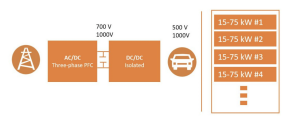
Figure 2 shows the simplified architecture of a fast DC EV charger. The two main components are an AC/DC three-phase power factor correction (PFC) or Active Front End (AFE) and a high-power isolated DC/DC converter. To provide the required capacity, high-power charging stations typically use multiple 15kW to 75kW sub-units.
Figure 2: Simplified architecture of a fast DC electric vehicle charger (source onsemi)
Each functional block can be implemented using a different topology—for example, a T-Neutral Point Clamp (T-NPC) for the PFC boost stage and a full-bridge LLC zero voltage switching (ZVS) for the DC/DC conversion.
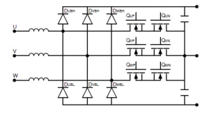
Figure 3 shows a typical three-phase PFC boost converter using 1,200-volt SiC MOSFET modules in a T-NPC topology.
Figure 3: A typical three-phase PFC stage using a T-NPC topology (source onsemi)
The dual active bridge topology implemented with half-bridge SiC MOSFET modules offers a space and energy-efficient arrangement for the DC/DC converter stage,
SiC Modules in EV Charging Infrastructure
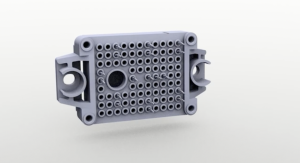
While the PFC and DC/DC converter stages can be constructed using discrete SiC MOSFETs, encapsulated SiC MOSFET power-integrated modules (PIM), have space and thermal management advantages. The onsemi NXH006P120MNF2PTG 2-pack SiC MOSFET module is an example of a half-bridge module that incorporates a 6mΩ RDS(on)1,200-volt MOSFET and a thermistor in a compact, thermally-efficient F1 package (see Figure 4).
Figure 4: The onsemi 1,200V, 10mΩ SiC MOSFET and integrated thermistor in an encapsulated thermally efficient F1 package (source onsemi)
This SiC half-bridge MOSFET module is designed for solar inverters, EV chargers, and industrial power applications.
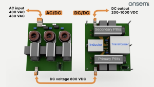
Figure 5 illustrates how NXH010P120MNF1 modules are used in the PFC and DC/DC converter stages of a 25kW EV charger. The 6-Pack PFC function (left) provides power factor correction and AC/DC conversion, boosting the DC input voltage to 800V for the DC/DC converter.
Figure 5: The functional architecture of a 25kW EV charger using onsemi NXH010P120MNF1 SiC MOSFET modules (source onsemi)
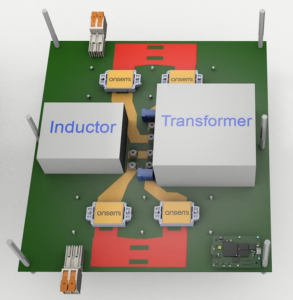
Figure 6 shows a dual active bridge with primary and secondary power integrated modules (without heatsinks or cooling fans). The DC/DC converter provides isolation between the vehicle and the three-phase supply and adjusts the output voltage and current levels for the EV’s battery management system.
The compact, low RDS(on), thermally optimised, and high-frequency characteristics of the onsemi SiC half-bridge modules make them suitable for high-power EV charging infrastructure applications.
SiC Modules Reduce Development Times for High Power Conversion Applications
The rapid deployment of reliable, fast-charging infrastructure will be a crucial driver for EV sales growth. This article showed that silicon carbide-based MOSFETs have superior characteristics compared to their silicon counterparts and how by packaging multiple MOSFETs into a compact, thermally optimised form factor, engineers can quickly bring the advantages of SiC to applications requiring high-power conversion.
Authored Article by:
Mark Patrick, Mouser Electronics

