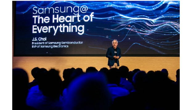
Samsung Electronics Co. presented its super gap roadmap for the next-generation semiconductor technology at the Samsung Tech Day 2018 in Silicon Valley on October 17.
The company disclosed the next-generation memory solutions based on the state-of-the-art technologies, such as the 10-nanometer (nm) class DRAMs and the sixth-generation NAND flashes.
It also announced that its foundry division has completed all process technology development and has started wafer production for its revolutionary process node, the 7-nm Low Power Plus (7LPP), which is based on extreme ultraviolet (EUV) lithography technology.
Samsung declared it has built a system to compete with Taiwan Semiconductor Co. (TSMC), the world’s largest contract chipmaker.
Samsung unveiled a raft of semiconductor innovations under the theme of “Samsung @ The Heart of Everything” at the Tech Day, which was held at Samsung Device Solutions America’s (DSA) building in Silicon Valley.
As the semiconductor fine process technology became more refined, fine circuit patterns have been realized by repeating the exposure process, or multi-patterning. However, semiconductors recently entered less than the 10-nm process, the conventional exposure process using argon fluoride (ArF) has reached the limit.
EUV is a light source of exposure apparatus that can replace ArF. It has less than one fourteenth of wavelength compared to conventional ArF. So, it is suitable to realize more elaborate semiconductor circuit patterns and allows to secure both semiconductors’ high performance and productivity at the same time by reducing multi-patterning complexity.
Samsung Electronics aims to secure the world’s highest competitiveness in the foundry industry by developing 3-nm process by 2020. The industry expects that Samsung will become one of the two large foundry companies, along with TSMC, which had sales of 36.5 trillion won (US$32.14 billion) and over 50 percent market share last year, when the new line starts operation. Samsung ranked fourth in terms of foundry market share with 7 percent as of last year.
The company also said it would provide new solutions like the key value SSD tailored to big data, smart SSD for artificial intelligence (AI) machine learning, and NVmEOF SSD combining storage with high-speed network SSD.
Samsung Electronics will hold a foundry form for European customers and partners in Munich, Germany, on the 18th (local time) after the U.S., China, South Korea and Japan and unveil its advanced process roadmap, including the 7-nm process.


