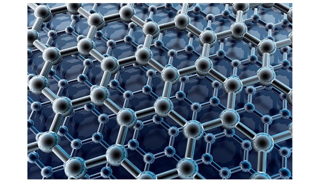
The shrinking of the electronic devices has proven that we may reach the limit of how smaller they can be made. Graphene, a carbon in the form of a single sheet of atoms arranged in a hexagonal lattice can make this possible. A unique demonstration of a new way of making transistors and logic gates from graphene, by employment of inorganic molecular dopants, has been made by a team of Indian Institute of Technology Bombay (IIT Bombay), in collaboration with Bhabha Atomic Research Center (BARC), Mumbai.
Electronic devices are made by using semiconductors like silicon, as the added dopants can control the electrical conductivity of semiconductors. Dominant charge carriers in the doped semiconductors could be positive or negative, depending on the dopants, making the material p-type or n-type. These two forms act as the fundamental building blocks for all further electronic and digital devices like the diodes and transistors. . In contrast to silicon, it is extremely difficult to control the dominant charge carrier and conductivity in graphene. While p-type graphene can be easily made, its n-type counterpart has been extremely challenging to realize and operate at ambient conditions.
A direct, one step and precise technique was used by the researchers of IIT Bombay, which neither requires high-temperatures nor vacuum to operate. Additionally, the resulting n-type graphene transistors have demonstrated stable operation for more than 10 months, in spite of being exposed to high temperatures (250⁰ C) and humidity levels (Relative Humidity 95%). The n-type graphene reported current density 1000 times higher than those in earlier devices.
Lanthanides are a class of inorganic elements that are widely used as catalysts in the chemical industry. Such materials have been investigated for applications pertaining to data storage. “We were interested in studying the synergy between Lanthanide-based molecules with two-dimensional nanomaterials”, explains Prof Maheswaran of IIT Bombay, who synthesized the lanthanide complex used as a dopant. The researchers themselves made the required compounds in their laboratory, instead of using commercially available chemicals. Thus they were able to experiment with the various compositions and create a compound that had the desired properties.
Precision microinjection needles are widely used in biomedical applications. Prof C. Subramaniam and his team dispensed the dopant on specific areas of graphene using precision micro-injection needles to create the n-type graphene transistors. Using these needles, the researchers could dispense the dopant on an area of 0.05 square millimetre on a 2 square millimetre graphene surface akin to painting a pinhead on a tennis court.
“The advantage of using an established technique is that it can be readily used without putting significant additional effort and it can easily be scaled for commercial production later; in fact, microneedle arrays are already commercially available”, comments Prof Subramaniam.
“This is a unique showcase of an interdisciplinary effort with electrical engineers and chemists working together to address a contemporary problem involving graphene transistors. This work paves way for the realization of basic circuit building blocks with the use of a novel doping methodology for graphene transistors” summarizes Prof. V. Ramgopal Rao, the Director of Indian Institute of Technology Delhi.


