Over the past decade or so, the semimetal graphene has attracted substantial interest among electronics engineers due to its many advantageous qualities and characteristics. In fact, its high electron mobility, flexibility and stability make it particularly desirable for the development of next-generation electronics.
Despite its advantageous properties, large-area graphene has a zero bandgap (i.e., the energy range in solid materials at which no electronic states can exist). This means that electric current in graphene cannot be completely shut off. This characteristic makes it unsuitable for the development of many electronic devices.
Researchers at Tsinghua University in China recently devised a design strategy that could be used to attain a larger bandgap in graphene. This strategy, introduced in a paper published in Nature Electronics, entails the use of an electric field to control conductor-to-insulator transitions in microscale graphene.
Since its discovery in 2004, graphene has attracted tremendous attention, owing to its single-atomic-layer thickness and high-mobility Dirac fermions. Due to these characteristics, graphene could find promising applications in the next generation electronics, especially when the rate of improvement in density and performance of silicon-based electronics is approaching the limit through dimensional scaling. However, large-area graphene is a semimetal with zero bandgap.
The on/off current ratio of conventional graphene-based field effect transistors (FETs) is approximately 30 at room temperature, which is far too low for logic device applications. To change graphene’s band structure and extend its bandgap, Zhang and his colleagues triggered a hydrogenation reaction, an electrochemical reaction that reversibly changes pristine graphene into highly-insulating hydrogenated graphene with a large transport gap.
The electrochemical graphene FETs can be cyclically switched on/off under the control of applied gate voltages, which demonstrates a new roadmap for the future application of graphene-based electronics.
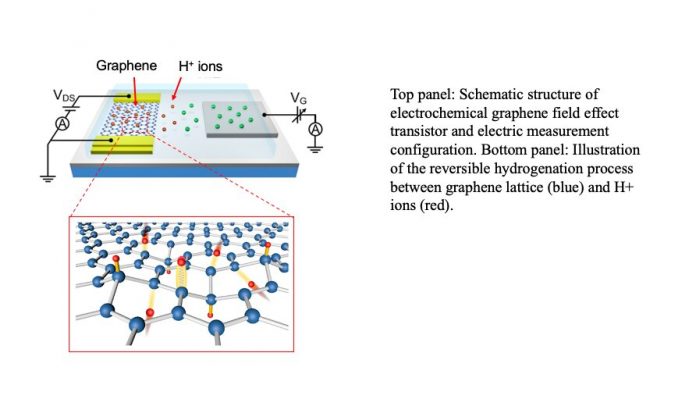
The graphene channels in the electrochemical FETs developed by the researchers were immersed in an organic liquid electrolyte with dissociative hydrogen ions (H+). When the researchers applied a positive gate voltage (VG) between the gate electrode (Pt foil) and graphene, the electric field caused H+ ions to accumulate on the FETs top surface.
When the VG is higher than the hydrogenation potential, the graphene lattice becomes highly activated and this triggers the chemical bonding between H+ ions and C atoms, which changes the hybridization of C-C bonds from sp2 to sp3, opening a huge bandgap in the electronic structure.
The primary advantage of the graphene-based FETs developed by this team of researchers is that they use highly versatile electric fields to control reversible hydrogenation reactions and switch the drain-source current. In addition, Zhang and his colleagues introduced a new hydrogen ion electrolyte that contains more dissociative H+ ions, which are also more reactive to graphene compared to electrolytes resulting from the hydrolysis of residual water in ionic liquid or in moister air.
By using the electric field control, we demonstrated the conductor–insulator transition in microscale graphene up to one million switching cycles. The sheet resistance of fully hydrogenated graphene shows a lower limit of 200 GW/sq, leading to a giant on/off current ratio larger than 108 in the graphene FETs at room temperature.
The electrochemical graphene FETs they created significantly outperformed similar devices fabricated in the past and exhibited a better on/off ratio, cycling endurance and switch time. Their work could inform the development of new graphene-based electronics and electric field-induced hydrogenation techniques to reversibly tune the atomic bonding and band structures of different 2D crystals.
This recent study could inspire other researchers to use similar strategies to seek out and identify new materials with desirable characteristics. The response time of the graphene-based FETs fabricated by these researchers is currently in the microseconds scale. In their next studies, however, Zhang and his colleagues would like to reduce this response time, so that their devices can be used across a broader range of applications.
In the future, we will focus on improving the response time by optimizing the device configurations, such as decreasing the distance between gate and source electrode, narrowing the width of graphene channel, and finding a better electrolyte with higher H+ ion conductivity. To make our devices more useful in the integrated graphene circuit, we will develop solid (or gel-like) electrolyte with high H+ ion conductivity and eventually downscale the size of our devices to micrometers.


