
In an exclusive interaction with ELE Times, Jaya Singh, Director – MSP WW Development at Texas Instruments, delves into the breakthrough innovations behind the world’s smallest MCU. She highlights how TI’s advanced packaging technologies, global collaboration, and the pivotal role of the India R&D team enabled unprecedented miniaturization without compromising performance or efficiency. This conversation also explores TI’s strategic roadmap, real-world applications, and the future of ultra-low-power microcontrollers in next-gen electronics.

ELE Times: What breakthrough technologies and design innovations enabled Texas Instruments to develop the world’s smallest MCU without compromising performance, power efficiency, or functionality?
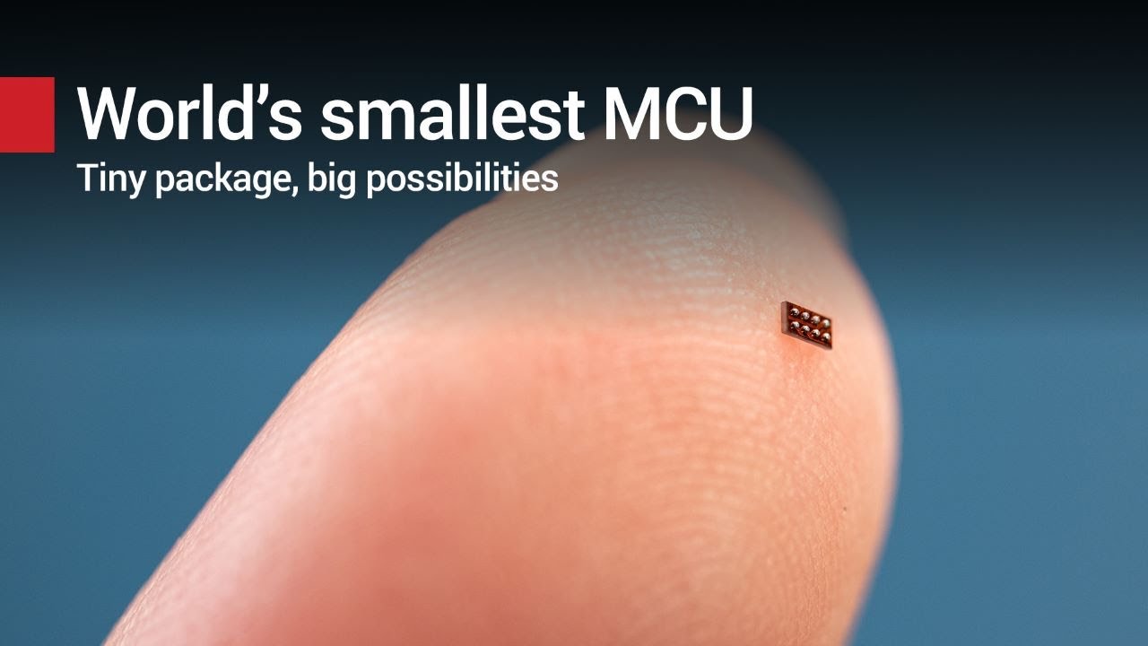
Jaya Singh: Despite its tiny size, the world’s smallest MCU offers robust features, including 16KB of flash memory, a 12-bit ADC with three channels, three timers, and 6 GPIOs. With an Arm® Cortex®-M0+ CPU running at 24 MHz, it empowers engineers to create compact, power-efficient designs without compromising on performance.


Texas Instruments achieved this by leveraging advanced wafer chip-scale packaging (WCSP) technology in combination with feature optimization efforts. WCSP offers the smallest possible form factor by directly connecting an array of solder balls to the silicon die, eliminating the need for a larger package. This results in a package size virtually equal to that of the silicon itself.
By fitting eight solder balls into a compact 1.38 mm² footprint, TI enabled higher feature integration per square millimeter. This miniaturization was further complemented by a deep understanding of customer needs, allowing TI to deliver a highly optimized embedded solution that balances size, cost, and functionality.
ELE Times: What role did TI India R&D team play in this development? Can you highlight their key contributions, collaboration with the global team, and the specific engineering challenges they helped overcome?
Jaya Singh: The TI India R&D team was involved in the complete lifecycle of the product, playing an instrumental role in the end-to-end development of the world’s smallest MCU. The India team played a vital role in defining the product specifications and ensuring a highly cost-optimized and efficient solution.
The India team collaborated closely with global teams, which enabled the integration of deep technical expertise with real-world application insights. This partnership helped overcome key engineering challenges, such as achieving ultra-small packaging without sacrificing functionality or reliability.
In parallel, the India team focused on tailoring the MCU to address the specific needs of customers. This included optimizing features such as memory configuration, analog peripherals and power efficiency to align with the demands of embedded systems used in industrial, automotive and consumer electronics sectors, such as those in India.
By combining technical leadership with market localization, the TI India R&D team ensured that this innovation not only set a global benchmark but also delivered practical value across key applications.
ELE Times: Cost optimization is critical in semiconductor design. How did TI achieve the right balance between affordability, energy efficiency, and high performance in this ultra-miniature MCU?
Jaya Singh: Achieving the optimal balance between cost, efficiency and performance required close collaboration across TI’s global engineering, design and manufacturing teams. This cross-functional effort enabled a holistic approach to cost optimization, ensuring that every element of the product was purposefully engineered for value.
Key innovations in manufacturing technology, packaging and circuit design played a pivotal role in making the MCU both compact and powerful.
ELE Times: What are some real-world applications where this MCU will be a game-changer, particularly in industries like wearables, medical devices, and ultra-low-power IoT?
Jaya Singh: As electrical circuits and system designs become smaller, board space is increasingly considered a scarce and valuable resource. TI’s MSPM0C1104 WCSP MCU enables innovation in size-constrained applications such as personal electronics, medical wearables, and factory automation. Using an ultra-small, feature-rich MCU in high-density designs enables engineers to design solutions with more room for additional components and larger batteries for increased operational lifetimes.
ELE Times: How does this innovation fit into TI’s broader roadmap for ultra-low-power and miniaturized semiconductor solutions, and what can we expect next in this space?
Jaya Singh: Since the launch of our Arm® Cortex®-M0+ MCU portfolio in 2023, Texas Instruments has rapidly expanded its offering to over 100 devices for industrial, medical and automotive systems. The portfolio offers scalable configurations of on-chip analog peripherals and a range of computing options, including other small packages to help reduce board size and bill of materials. We support the portfolio with a comprehensive ecosystem of hardware and software resources, to help engineers reduce system cost and complexity while meeting diverse application needs. In the future, we plan to continue expanding the portfolio to meet the growing needs of the industry.
The introduction of the world’s smallest MCU demonstrates TI’s commitment to developing small packages across our embedded processing and analog portfolio that help our customers innovate in size-constrained applications. The trend of smaller, more compact design requirements will continue to grow. Packaging advancements enable engineers to integrate more functionality into smaller form factors while maintaining high levels of precision and performance, enhancing user experiences and creating new design possibilities.
TI’s investments in internal manufacturing and technology have given the company greater control of its entire manufacturing process, while also lowering costs. By optimizing packaging solutions for specific application needs, TI can explore new design approaches and technologies while achieving the highest levels of quality and reliability – driving innovation and meeting changing industry demands.
ELE Times: With semiconductor technology constantly evolving, what unique challenges and opportunities do you foresee in pushing the boundaries of MCU miniaturization further?
Jaya Singh: With each new generation of electronics, consumers expect continuous advancements in size and functionality. To meet these demands, engineers are challenged to add new features while maintaining or decreasing their products’ current form factors. TI is committed to helping our customers overcome their design challenges and get to market quickly with MCUs that are scalable, cost-optimized and easy-to use.