


Courtesy: Lam Research
- The tool enables the deposition of high-quality, highly scandium-doped AlScN films
- Features include dual-chamber configuration, degas, preclean, target library, precise laser scanning, and more
In this post, we explain how the Pulsus system works, and how it can achieve superior film quality and performance compared to conventional technologies.


PiezoMEMS devices are microelectromechanical systems that use piezoelectric materials to convert electrical energy into mechanical motion, or vice versa. They have applications in a wide range of fields, including sensors, actuators, microphones, speakers, filters, switches, and energy harvesters.
PiezoMEMS devices require high-quality thin films of piezoelectric materials, such as aluminum scandium nitride (AlScN), to achieve optimal performance. Conventional deposition technologies—think sputtering or chemical vapor deposition—face challenges in producing AlScN films with desired properties, such as composition, thickness, stress, and uniformity. These obstacles limit both the scalability and functionality of piezoMEMS devices.
Revolutionary Tech
To help overcome these challenges, Lam Research recently introduced Pulsus, a pulsed laser deposition (PLD) system that we hope will revolutionize the world of piezoMEMS applications. The addition of Pulsus PLD to the Lam portfolio further expands our comprehensive range of deposition, etch and single wafer clean products focused on specialty technologies and demonstrates Lam’s continuous innovation in this sector.
Pulsus is a PLD process module that has been optimized and integrated on Lam’s production-proven 2300 platform. It was developed to enable the deposition of high-quality AlScN films, which are essential to produce piezoMEMS devices.
A key benefit of the Pulsus system is its ability to deposit multi-element thin films, like highly scandium-doped AlScN. The intrinsic high plasma density—in combination with pulsed growth—creates the conditions to stabilize the elements in the same ratio as they arrive from the target. This control is essential for depositing materials where the functionality of the film is driven by the precise composition of the elements.
Plasma, Lasers
Local plasma allows for high local control of film specifications across the wafer, like thickness and local in-film stress. Pulsus can adjust deposition settings while the plasma “hovers” over the wafer surface. This local tuning of thickness and stress allows for high uniformities over the wafer, which is exactly what our customers are asking for. And because the plasma is generated locally, Pulsus uses targets that are much smaller than you would typically see in PVD systems. Pulsus can exchange these smaller targets, without breaking vacuum, through a target exchange module—the target library.
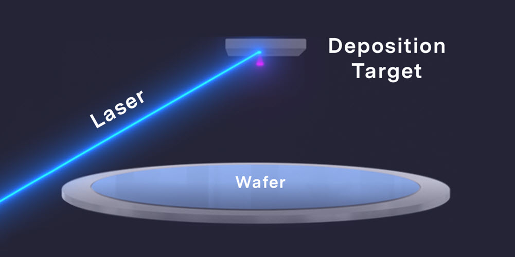
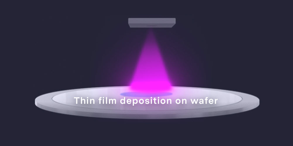
Pulsus uses a pulsed high-power laser to ablate a target material, in this case AlScN, and create a plasma plume. The plume expands and impinges on a substrate, where it forms a thin film.
Pulsus has a fast and precise laser optical path which, in combination with the target scanning mechanism, allows for uniform and controlled ablation of the target material. The Pulsus system has a high control of plasma plume generation, wafer temperature, and pressure control to achieve the desired film composition and stoichiometry.
By combining these features, Pulsus can produce high-quality films with superior performance for piezoMEMS devices. Pulsus can achieve excellent composition control, with low variation of the scandium (Sc) content across the wafer and within individual devices. It also delivers high film uniformity, with low WiW (within-wafer) and wafer-to-wafer (WtW) variation of the film thickness and stress.
Breakthrough Technology
Pulsus is a breakthrough technology for AlScN deposition, which can improve film quality and performance for piezoMEMS applications. In addition, Pulsus has the potential to enhance the functionality and scalability of piezoMEMS devices. The Pulsus technology deposits AlScN films with very high Sc concentration, resulting in high piezoelectric coefficients, which drive higher device sensitivity and output. These films feature tunable stress states to enable the design of different device configurations and shapes.
Pulsus is currently in use on 200 mm wafers and is planned to expand to 300 mm wafers in the future—a move that has the potential to increase the productivity and yield of piezoMEMS devices.