ELE Times : Tell us about your recent work on Photonics (Mid-IR integrated photonic devices)?
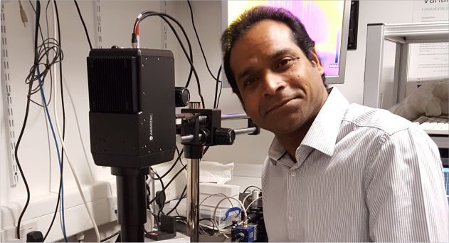
Dr. Senthil Ganapathy : Currently I am developing integrated photonic devices made of Mid-Infrared materials. These materials and devices are transparent to the infrared light and therefore, by integrating many device functionalities on one chip we can perform same or better experiments and analyses carried out by huge infrared spectrometers.
Biochemical analysis for medical diagnostics is normally carried out by trained operators in sophisticated laboratories using large instruments. These techniques are out of reach to many people living in remote areas or are too slow for critically ill patients who need urgent care. The device we are developing will simplify this issue and can provide accurate and reliable information rapidly by exploiting the mid-infrared molecular finger-print detection and requires only very low volume of sample for analysis. Since this technology is based on mass production approaches these chips could be produced at very low cost affordable to a common man. Novel material platform which is transparent in the whole infrared window of interest have been developed and optical circuits were fabricated and tested for this special lab-on-a-chip sensor applications. Currently sensitivity is being optimised on these optical circuits using model chemical molecules and integration of various functionalities on a same chip is being designed and efforts are underway to fabricate them.
ELE Times : What are the materials you have worked in photonics for sensing applications and what is the reason behind it?
Dr. Senthil Ganapathy : For sensing applications (especially Mid-IR lab on a chip) we are exploiting a special category of materials called Chalcogenides. These are materials based on Sulphur, Selenium and Tellurium. We have demonstrated photonic circuits made of Germanium Telluride (GeTe4) and Zinc Selenide (ZnSe). The main reason why we have chosen these materials was their transparency in the whole Mid-IR spectral region together with their high refractive index which is essential to achieve high sensitivity. We have used silicon wafer as a substrate to fabricate these photonic circuits as it is a convenient substrate for microfabrication and mass production.
ELE Times : What are the challenges in working with Mid-IR integrated photonic devices and remedy for it?
Dr. Senthil Ganapathy : The main challenge working with Mid-IR photonic devices is the availability and affordability of test and measurement tools in the Mid-IR spectral region. Test and measurement tools and optics in the near-infrared (NIR) region is well established and are cheap as the telecommunication wavelength band lying in the NIR region which creates a huge market for such tools. Whereas the Mid-IR spectral region was mainly exploited in the past only for military and security purposes, only very recently it has been very actively researched for various other applications including molecular finger print sensing and the test and measurement tools in the Mid-IR is only starting to evolve. Keeping this need in mind I have recently established a major Mid-IR characterisation facility, worth about £1M, which is unique for waveguide characterisation and spectroscopy in the Mid-IR (2-14 μm) spectral region.


