When designing a system that requires high channel density such as in test instrumentation, there is typically a necessity to include a large number of switches on the board. When using switches controlled by a parallel interface, a large percentage of board space is taken up by the logic lines necessary to control the switches, as well as the serial-to-parallel converters needed to generate the GPIO control signals. This articles discusses the new generation of ADI SPI controlled switches that address this design challenge, their architecture, and the channel density increase they offer vs. parallel controlled switches. ADI’s innovative copackaging process enables a new SPI-to-parallel converter die to be combined with existing high performance analog switch die. This allows space saving to be offered without compromise to the precision switch performance.
Maximizing channel count in test equipment is of the utmost importance, as this allows more devices to be tested in parallel, which, in turn, cuts testing time and cost for the end customer. Switches are a key element in allowing channel increases, as they enable the tester to share its resources to support multiple DUTs. But more parallel controlled switches means more control lines, resulting in increased board space consumed. This severely restricts the channel density that can be realized.
Using SPI controlled switches in this situation offers significant benefits in terms of solution size and channel count. The SPI switches can be placed in a daisy-chain formation that massively reduces the number of digital lines needed as compared to a traditional solution.
This article details the problems encountered when trying to maximize channel count, discusses the traditional method used to control a group of switches and the associated drawbacks, presents the solution offered by SPI controlled analog switches, and finally introduces the best-in-class performance, SPI controlled ADI precision switches.
Common Issues When Maximizing Channel Count
When developing a module where the main aim is to maximize channel count, board space becomes a commodity. Switches are key to increasing channel count in a system but as the number of switches increase, board space is reduced not only by the switches themselves, but by the logic lines and associated devices needed to generate these logic lines. Ultimately the channel count that can be realized suffers because of the associated items needed to control the switch itself.
Traditional Parallel Switch Solution
The most common solution to increasing channel density is to use switches that are controlled by parallel logic signals. This requires a large amount of GPIO signals that a standard microcontroller would not be able to supply. A solution to generating the GPIO signals is using serial-to-parallel converters. These devices output parallel signals and are configured by serial protocols such as I2C and SPI.
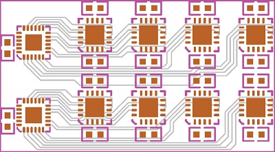
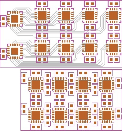
Figure 1 is a layout, showing eight ADG1412 quad, single-pole single-throw (SPST) switches in a 4 × 8 cross point configuration on a 6-layer board. The switches are controlled by two serial-to-parallel converters with the serial lines coming from a controller board. Each converter supplies 16 GPIO lines each that are distributed between the eight switches. The layout shows the footprints of the devices, supply decoupling capacitors, and the digital control signals in gray. The size of 4 × 8 matrix solution using the parallel controlled switches is 35.6 mm × 19 mm, which Occupies an area of 676.4 mm.2
As is evident from Figure 1, a large percentage of the solution area is taken up by the serial-to-parallel converters and the digital control lines, rather than the switches themselves. This inefficient use of board space is not ideal and will vastly reduce the number of switches in the module, which, in turn, has a detrimental effect on the channel count of the system.
SPI Switch Solution
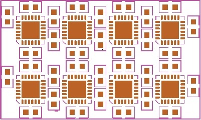
Figure 2 shows a 4 × 8 cross point configuration with eight quad SPST switches on a 6-layer board. However, this time the switches are SPI controlled ADGS1412 devices. As before, the device footprints, supply decoupling capacitors, and SDO pull up resistors are shown.
The solution shows the devices configured in a daisy-chain formation. All device share the same chip select and serial clock digital lines from an SPI interface, while the first device in the chain receives the serial data. This data is then passed through all devices in the chain like a shift register. The size of this example solution is 30 mm × 18 mm, which is an area of 540 mm.2
The use of the SPI interface in a daisy-chain format vastly reduces the board space occupied by the serial-to-parallel converter and the digital lines. So much so that an overall board area reduction of 20% is realized with the same switch configuration. This enables a large increase in channel density. The system platform is also simplified. When the switch count increases on a board, the space area savings ramps up along with that—leading to >50% space saving on boards containing hundreds of switches.
This demonstrates the ability to fit more switches into a smaller area, which in turn would allow for the large channel count on a fixed area board compared to the traditional serial-to-parallel converter solution.
ADI SPI Switch Features
ADI’s new SPI switch portfolio can be used to achieve increased channel density, as shown in the previous example. An innovative stacked dual-die solution (Figure 4) enables ADI’s current industry-leading precision switches to be configured with an industry standard, SPI mode 0 interface. This means that the space saving can be achieved without having an adverse effect on the performance of the system. The following is a summary of the key functionality of the new ADI SPI switch.

Daisy-Chain Mode
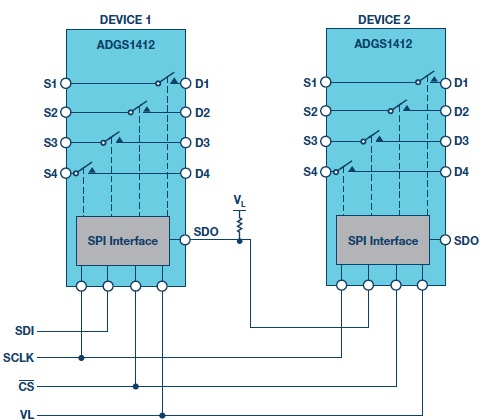
As outlined before, the ADI SPI switches are able to operate in daisy-chain mode. The connection of ADGS1412 devices in a daisy-chain is illustrated in Figure 5. All devices share CS and SCLK digital lines, whereas the SDO of a device forms a connection to the SDI of the next device. One single 16-bit SPI frame is used to command all the devices in the chain to enter daisy-chain mode. In daisy-chain mode, SDO is an 8-cycle delayed version of SDI, so the desired switch configuration can be passed from one device to the next device in the chain.
Error Detection Function
When the device is in address mode or burst mode, protocol and com-munication errors on the SPI interface are detectable. There are three error detection methods, which are incorrect SCLK count, invalid read and write address, and CRC error detection up to 3 bits. These error detection function ensure a robust digital interface even in the harshest of environments.
ADI SPI Switch Family
The ADGS1412 is the first release in a family of SPI switches that are being developed by Analog Devices. Thanks to the innovative dual-die solution developed by ADI, the ADGS1412, has the same best-in-class, low RON performance as the parallel controlled ADG1412 while offering the benefits that a serial interface brings.
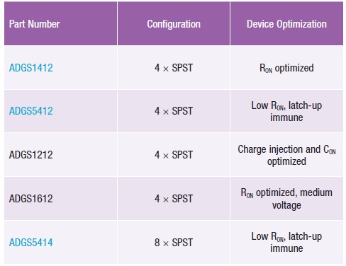
The portfolio will be built on ADI’s high performance switches, offering SPI controlled versions of the industry-leading switches already available. Table 1 shows the current and planned products in the new ADI SPI switch family. The part number represents which analog switch die is co-packaged with the SPI-to-parallel converter with an additional S to show that this is the SPI controlled version. These products will be released throughout 2017.
Summary
Using SPI controlled switches in a high channel density application has many advantages over the use of parallel controlled switches. It enables the reduction of board space used per switch, which in turn increases the density of switches that can be realized. This is due to the reduction of digital control lines needed and the removal of the devices required to provide these control lines.
Analog Devices has a new innovative precision SPI switch solution that enables the increase of channel density. This is facilitated by the daisy-chain mode that is available on these devices. The same industry-leading switch performance seen in Analog Devices’ current switch offerings is maintained due to the dual-die solution used. The ADGS1412 is the first release in a family of new SPI controlled switches with a complete portfolio coming in 2017 and 2018.
Stephen Nugent Bio:
 Stephen Nugent is an Applications Engineer in the Linear and Precision Technology Group of Analog Devices. He graduated from Queen’s University Belfast in 2014 with a Master’s Degree in Electrical and Electronic Engineering. Stephen joined the Linear and Precision Technology Group in July 2014 supporting the analog switch and multiplexer product portfolio. He also previously worked in the Precision Converter Group within ADI.


