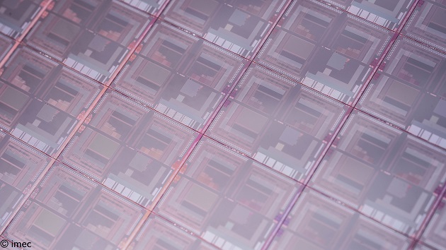
Imec has developed a thin-film monolithic image sensor that captures light in the near-infrared (NIR) and short-wavelength infrared (SWIR).
Based on a monolithic approach, the process promises an order of magnitude gain in fabrication throughput and cost compared to processing today’s conventional IR imagers, while at the same time enabling multi-megapixel resolution.
To date, infrared image sensors are produced through a hybrid technology: the crystalline semiconductor detector and the electronic readout are fabricated separately and then interconnected at pixel or chip periphery level.
This is an expensive and time-consuming process with a low throughput, resulting in sensors with a restricted resolution that often require cooling to reduce the signal noise under dark conditions.
This prevents a widespread use of IR imagers in consumer applications. For some time, researchers have been looking at various monolithic approaches. Imec’s approach paves the way to high-resolution, low-cost, wafer-based SWIR imagers.
Imec’s IR imagers consist of a thin-film photodetector pixel stack based on quantum dots deposited directly on top of an electronic readout.
They are manufactured in a monolithic process compatible with wafer-based mass production.
The pixels embed newly developed high-performance low bandgap quantum dot materials that match or even surpass the performance of inorganic light absorbers. The stacks have been carefully engineered and can be tuned to target a spectrum from visible light all the way up to 2µm wavelength.
Test photodiodes on silicon substrate achieve an external quantum efficiency above 60 percent at 940nm wavelength, exceeding the state-of-the-art, and above 20 percent at 1450nm, allowing for uncooled operation with dark current comparable to commercial InGaAs photodetectors.
The prototype imager has resolution of 758×512 pixels and 5um pixel pitch.


