Overview
Many test and measurement applications call for the timing and synchronization of multiple instruments because of the limited number of stimulus/response channels on a single instrument and/or the need for mixed-signal stimulus/response channels. For example, an oscilloscope may have up to four channels and a signal generator up to two channels. Applications ranging from mixed-signal test in the electronic industry to laser spectroscopy in the sciences require timing and synchronization (T&S) for higher-count channels and/or the need to correlate digital input and output channels with analog input and output channels.
Timing and Synchronization in Applications
In the electronics industry, mixed-signal test is an important aspect of testing devices and system on chip (SOC) technology. With the convergence of audio, video, and data in consumer electronics and communications, the need for test of such technology from baseband to RF requires precise T&S.
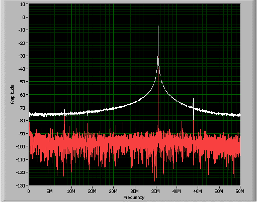
Mixed-signal devices, in essence, contain multiple digital and analog channels. These channels are often tested at the same time in an ATE system to minimize test time and increase throughput. Additionally, the analog channels are tested with coherent sampling instrumentation systems. Coherent sampling systems call for the synchronization of heterogeneous clocks in analog-to-digital conversion (ADC) and digital-to-analog conversion (DAC) test. This synchronization is highly desired to minimize spectral leakage in frequency-domain measurements. The following LabVIEW graph illustrates the effect of noncoherent sampling vs coherent sampling. The white trace corresponds to noncoherent clocking whereby a fractional number of cycles of the analog sine wave are captured. The spectrum leakage in the FFT leads to “skirts” in the spectrum. With the same sampling rate, a coherent sampling system leads to the red trace. One of the key benefits of coherent sampling is the reduction of test times because of shorter signal acquisition times. Shorter acquisition times are attained by not having to capture extra signal cycles to which to apply a digital window for elimination of the spectral leakage.
In principle, an ATE system designed to meet the flexible needs of the wide variety of devices in the marketplace should deliver instrumentation with clocks that are different but derived from a master reference clock for coherent sampling. Additionally, this system should be able to deliver arbitrary clock frequencies derived from a master reference clock.
Figure 1. NI-TClk synchronization of the NI PXI-5421 arbitrary waveform generator and NI PXI-5122 digitizer delivers phase-coherent stimulus-response measurements with higher accuracy and shorter test times.
In communications, analog and digital baseband I/Q signal generation and acquisition require phase offset accuracy and control. A digital pattern generator/analyzer is synchronized with an arbitrary waveform generator and a digitizer to address digital and analog I/Q signal generation and acquisition. The accuracy and control requirements of phase and gain offset between each channel can be as low as 0.003% and 0.1%, respectively, for signals with bandwidths that approach 5 MHz in 3G W-CDMA schemes, for example. In future 4G communication schemes, such as multiple-input multiple-output (MIMO) antenna systems, requirements for multiple-channel baseband, IF, and RF signal generation and acquisition with tight synchronization will be critical. Digital beam forming, an emerging technology, is playing into multiple applications from 4G MIMO communications to radar applications in defense and aerospace industries. Digital beam forming requires multichannel phase-coherent digitizing systems with digital downconversion engines.
In the semiconductor industry, functional digital test can consume up to 1000 digital pins. Typical integrated circuits (ICs) on the market can take somewhat less than 200 pins of digital I/O. In such an application, multiple digital pattern generators and analyzers are synchronized with the requisite pin-to-pin skew and jitter to address high-pin-count ICs.
In consumer electronics, component digital video signal generation and acquisition may require up to five distinct signals: the three primary video signals, H-Sync, and V-Sync. With T&S, arbitrary waveform generators and digitizers can be synchronized to generate and acquire high-definition video signals respectively, with pixel rates that can approach 165 MHz. CMOS imaging sensors, a technology expected to become mainstream with the prevalence of camera phones and digital cameras, is an example of mixed-signal technology whereby an arbitrary waveform generator, digitizer, and digital pattern analyzer are synchronized for design validation and verification of the chip or chip set.
In the physical sciences, high-channel-count digitizing systems are used in plasma-fusion, laser-scattering experiments, and photon/particle detection and tracking in particle and astrophysics. In these examples, high-channel-count digitizing systems are used for 2D or 3D reconstruction of temporal and spatial phenomena. Such applications call for simultaneous sampling of multiple channels, extending from a few channels to over several hundred.
In medical diagnostic systems, 3D digital-imaging systems are fast replacing analog systems since the advent of cost-effective 12 and 14-bit 50 MHz ADCs. Such systems typically scale from a hundred to over a thousand channels. In nondestructive test, 3D ultrasonic imaging is realized with multichannel systems that include 50 MHz digitizers. Optical coherence tomography (OCT), a relatively new imaging method compared to ultrasonic imaging, can require several digitizer channels as well to interface to multiple photodiodes for coherent sampling.
As can be seen from the many applications, T&S technologies will be an important element to multichannel signal/data generation and acquisition.
The National Instruments Platforms for Modular Instrumentation
Today, National Instruments hardware platforms for modular instrumentation are PXI [3] and PCI. Both platforms are modular in nature and use the PCI bus to interface between the PC and the instrument.
Introduced in 1997, PXI is an open standard with many vendors who offer a wide range of PXI modules from image acquisition to RF vector signal analyzers. PXI has been gaining rapid acceptance because of its relatively small package, portability, high throughput using the PCI bus, and lower costs, which are made possible through use of standard commercial technologies spawned by the large PC industry.
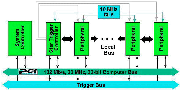
Electrically, PXI extends the CompactPCI standard by adding local buses and synchronization features. For synchronized measurements, key elements built into PXI are the reference clock, the trigger bus, and the star trigger bus.
Figure 2. Illustration of the PXI Timing and Triggering Extensions to the CompactPCI Platform
| Local Bus | Triggers | Clock | Star Trigger Bus | |
| PXI | 13 lines | 8 TTL | 10 MHz TTL | 1 per slot |
Building Blocks for Synchronization
To achieve synchronization across multiple devices, you need to examine the distribution of clocks and triggers. There are two main schemes for synchronization, but before we examine the schemes we need to define the following terms.
Sample Clock, Reference Clock, Triggers, and Master and Slave Devices
Names of signals used for synchronizing measurement devices are not standardized and may vary with device type and manufacturer. This paper uses the following terms in reference to high-speed measurement devices to illustrate different types of signals used to control measurements.
- Sample clock is a signal that controls the timing of the analog-to-digital and digital-to-analog conversions performed by the ADC and DAC on digitizers and signal generators respectively. The sample clock is also the signal that controls the rate at which digital waveforms are acquired or generated on digital pattern generators/analyzers. The sample clock is most often a periodic signal, derived from a crystal oscillator on the device. Various crystal oscillator technologies include voltage-controlled crystal oscillators (VCXOs), temperature-controlled crystal oscillators (TCXOs), and oven-controlled crystal oscillators (OCXOs).
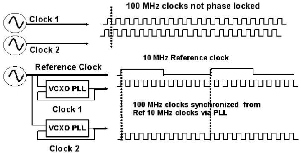
- Reference clock – Many instruments contain phase-lock loops (PLLs). A PLL can lock the frequency of its output to a reference clock at its input. In instruments, a common frequency is 10 MHz, although many instruments allow a variety of reference-clock frequencies. The output of the PLL is typically the sample clock. Using a PLL, the sample clock frequency can be locked to the reference clock frequency. Therefore the absolute frequency accuracy of the sample clock will be identical to the frequency accuracy of the reference clock.
- Trigger signals control data acquisition at the highest level. External events or triggers are the main methodologies for initiating an acquisition and generation. Triggers come in different forms, including analog, digital, and software.
- Master and Slave Devices – When creating synchronized measurement systems, you typically designate one device as a master and one or more other devices as slaves. The master device is the device that generates a signal or signals used to control all the measurement devices in the system. The slave devices receive control signals from the master device.
The goal of synchronization is to generate and/or receive analog and digital signals precisely among multiple hardware devices. One class of T&S is referred to as homogeneous timing and synchronization – two identical devices with identical settings generating and or acquiring signals with a precise phase relationship between each sample clock, starting at the same instant in time. The following example illustrates homogeneous synchronization:
- Two digitizers acquire data at 200 MS/s with a precise phase relationship between each sample clock, triggered at the same instant in time, with identical vertical gain settings, AC/DC coupling settings, input impedance settings, DC offset settings, and analog filter settings.
An important observation from the previous example is the relevance of many settings to homogenous synchronization. The delays of gain stages and analog filters on the front end of a digitizer lead to a time delay from the front end connector to the ADC, for example.
Heterogeneous synchronization can imply many different scenarios. Some following examples illustrate heterogeneous synchronization:
- Two digitizers acquire data at 200 and 100 MS/s respectively with a precise phase relationship between each sample clock, triggered at the same time, with identical vertical gain settings, AC/DC coupling settings, input impedance settings, DC offset settings, and analog filter settings.
- An arbitrary waveform generator and digitizer sampling at 100 MS/s with a precise phase relationship between each sample clock and with a set time delay in start of operation, upon reception of an incoming trigger signal.
- A digitizer, digital pattern generator/analyzer, and arbitrary waveform generator sampling at 50, 200, and 100 MS/s, respectively with a precise phase relationship between each sample clock, and with a defined time delay in start of operation, upon reception of an incoming trigger signal.
The preceding examples clearly show that heterogeneous T&S imply a wide range of possibilities to address the application needs. Separate settings on each device can lead to delays of data/signals being sampled at the same instant in time. The key is calibration of the synchronized system, which will be discussed later in this paper.
Synchronization Scheme 1 – Synchronization with a Sample Clock
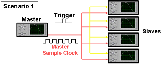
The master device can control operation of the measurement system by exporting both trigger signals and a sample clock to the slave devices. For example, a system comprised of multiple digitizers and signal generators has a common sample clock from an appointed master device. As illustrated in Figure 3, the master sample clock directly controls ADC and DAC timing on all devices. For example, National Instruments dynamic signal analyzers such as the NI 4472 and NI 4461 (24-bit 104 kS/s and 208 kS/s respectively) are synchronized using this technique for applications in sound and vibration measurements.
This scheme is the purest form of phase-coherent sampling; multiple devices are fed the same sample clock. Thus the same accuracy, drift, and jitter of the sample clock are seen by every device. The disadvantage of this scheme is that it does not address all possible phase-coherent heterogeneous clocking needs.
Figure 3. Synchronization with a Sample Clock
Synchronization Scheme 2 – Synchronization with a Reference Clock
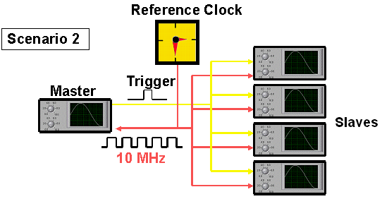
Synchronization can be implemented by sharing triggers and reference clocks between multiple measurement devices. In this scheme, the reference clock can be supplied by the master device if it has an onboard reference clock, or the reference clock can be supplied by a dedicated high-precision clock source.
This advantage of this scheme is that with it you can derive heterogeneous sample clocks from a single reference clock to which all the sample clocks phase locked. The trade-off is that the phase-coherent sampling on each device is not as pure as the direct sample clock approach, because each device clock enters the picture, so device clock jitter must be considered.
The method usually employed with this scheme to synchronize and generate sampling clocks is a PLL.
Figure 4. Synchronization with a Reference Clock
Figure 5. High-speed sample clocks are synchronized using a PLL.
Issues with Synchronization
Distributing clocks and triggers to achieve high-speed synchronized devices is beset by nontrivial issues. Latencies and timing uncertainties involved in orchestrating multiple-measurement devices are significant challenges in synchronization, especially for high-speed measurement systems. These issues, often overlooked during the initial system design, limit the speed and accuracy of synchronized systems. Two main issues that arise in the distribution of clocks and triggers are skew and jitter.
Sample Clock Synchronization
Mixed-signal test by its nature requires different sampling rates on each instrument, because analog waveform I/O and digital waveform I/O necessitate different sampling rates. But they need to be synchronized, and more importantly data needs to be sampled on the correct sample clock edge on each instrument.
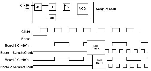
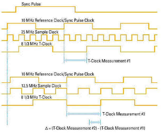
When sample clocks on disparate instruments are integer multiples of the 10 MHz reference clock, all instruments will have sample clocks that are synchronous to each other – the rising edge of all sample clocks will be coincident with the 10 MHz clock edge. When sample clocks are not integer multiples, such as 25 MHz, there is no guarantee that the sample clocks are in phase, despite being phase-locked to the 10 MHz reference clock, as shown in Figure 6. Standard techniques are used to solve this problem by resetting all of the PLLs at the same time, leading to sample clocks of the same frequency being in phase, as shown in Figure 7. Even though all sample clocks are in phase at this point, the solution is still not complete. Perfect synchronization implies the data clocked from device to device corresponding to within a sample clock cycle. The key to perfect synchronization is triggering, which will be discussed later.
Figure 6. 25 MHz Sample Clocks Not Aligned
Figure 7. PLL Synchronization with Reset
Clock Skew and Jitter
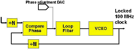
The distribution of the sample clock or the reference clock requires careful planning. For example, a synchronized measurement system calls for simultaneous sampling of 20 channels at 200 MS/s. This requirement implies distributing a clock to 10 two-channel digitizers. For a sample clock skew of 1%, the skew must be under 25 ps. Such a system certainly looks very challenging. Fortunately, skew limitations can be dealt with by calibrating the skew to each measurement device; you can compensate for the skew in the sampled data. The real issue is the clock frequency. Distributing either a 200 MHz direct sample clock or a 10 MHz reference clock introduces jitter into the system. The physical properties of the distribution system play a significant role in the accuracy of the distributed clocks; if the clock paths are susceptible to high-frequency electrical noise then clock jitter becomes a significant problem. Producing a platform for distribution of high-frequency sample clocks becomes expensive in terms of the manufacture, test, and calibration. Thus synchronization through the use of lower frequency reference clocks is the preferred method in many high-frequency systems. Figure 8 is a typical VCXO PLL implemented on National Instruments SMC-based modular instruments. The loop bandwidth is kept at a minimum to reject the jitter coming from the reference clock, while the VCXO on the device has jitter less then 1 psrms. Such a system effectively realizes a low-jitter synchronized system.
A very useful property of the National Instruments PLL design is the use of a phase DAC. Using a phase DAC, you can phase-align the output of the VCXO with respect to the incoming reference clock. Nominally the VCXO output is in phase with the reference clock; however, you may need to skew the VCXO output slightly to place the output out of phase by a small margin. This feature is important for aligning sample clocks on multiple devices when the reference clock fed to each device has a small skew due to propagation delays. For example, in the NI PXI-1042 PXI chassis, the distribution of 10 MHz reference clock has slot-to-slot skew of 250 ps maximum with a maximum of 1 psrms jitter. Slot-to-slot skew of 250 ps, while satisfactory for most applications, may not be adequate for very high-speed applications where phase accuracy is important. To overcome this skew, the phase DAC outputs can be adjusted to calibrate for the skew. On the NI PXI-5422, 200 MS/s arbitrary waveform generator and NI PXI-5124 200 MS/s digitizer the sample clock phase/delay adjustment is 5 ps, thus giving the user significant flexibility in synchronizing multiple devices.
Figure 8. PLL with Phase Adjustment DAC for Flexibility in Sample Clock Delay with Respect to the Reference Clock
Trigger Skew and Distribution
With sample clock synchronization addressed, the other main issue is the distribution of the trigger to initiate simultaneous operation. The trigger can come from a digital event or from an analog signal that meets trigger conditions. Typically in multichannel systems, one of the devices is made the master and the rest are designated as slaves. In this scenario, the master is programmed to distribute the trigger signal to all slaves in the system including itself. Two issues that arise here are trigger delay and skew. A trigger delay from the master to all the slaves and skew between each slave device is inevitable, but this delay and skew can be measured and calibrated.
The challenge in measuring the delay and skew, however, is a two-part process:
- Automate the measurement of the trigger delay between master and each slave and compensate for it.
- Ensure that the skew between slaves is small enough to ensure that the trigger is seen on the same clock edge on all devices.
The distribution of the trigger signal across multiple devices requires passing a trigger signal into the clock domain of the sample clock such that the trigger is seen at the right instance in time on each device.
With sample clock rates less than or equal to 100 MS/s, skew becomes a major obstacle to accurate trigger distribution. A system consisting of ten 200 MS/s devices, for example, requires a trigger being received at each device within a 5 ns window. This places a significant burden on the platform for delivering T&S beyond 100 MHz. The trigger signals must be sent in a slower clock domain than that of sample clock, or you must create a nonbused means of sending the trigger signal (such as a point-to-point connection). The costs of such a platform become prohibitive for mainstream use. Another distribution channel is needed; the trigger signal needs to be distributed reliably using a slow clock domain and transferred to the high-speed sample clock domain. A logical choice is to synchronize the trigger signal distribution with the 10 MHz reference clock. However, this cannot ensure that two boards will see the trigger assertion in the same sample clock cycle when the sample clocks are not integer multiples of the 10 MHz reference clock. To illustrate this point, assume two devices have the simple circuit [4] shown in Figure 9 for trigger transfer from the 10 MHz reference clock domain to the sample clock domain.
Figure 9. 10 MHz Reference Clock Domain to Sample Clock Domain Trigger Transfer
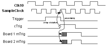
Even if the sample clocks of the devices are aligned, the following timing diagram shows why the trigger may not be seen in the same sample clock cycle on both devices.
Figure 10. Effect of Metastability on Triggers
The output of the first flip-flop (cTrig) may occur too close to the rising edge of the sample clock, causing mTrig to be metastable. When the metastability finally settles, it may do so differently on different devices, causing them to see the same trigger signal at two different instants in time.
SMC Modular Instrumentation and NI-TClk
In 2003, NI introduced the first series of PXI digitizers, arbitrary waveform generators, and digital pattern generators/analyzers based on the Synchronization and Memory Core (SMC) foundation [5]. One of the key technologies implemented on the SMC was NI-TClk (pronounced T-Clock) technology for T&S applications.
NI-TClk
NI has developed a method for synchronization whereby another signal-clock domain is employed to enable alignment of sample clocks and the distribution and reception of triggers. The objectives of NI-TClk technology are twofold:
- NI-TClk aligns the sample clocks that may not be necessarily aligned initially despite being phase locked to the 10 MHz reference clock.
- NI-TClk enables accurate triggering of synchronized devices.
NI-TClk synchronization is flexible and wide ranging; it can address the following use cases:
- Extension of synchronization from a single PXI chassis to several PXI chassis to address large channel systems using the NI PXI-6653 Slot 2 system timing and control module.
- Homogeneous and heterogeneous synchronization – devices running at the same or different sample rates, using internal or external sample clocks.
- NI-TClk synchronization can be used with both Schemes 1 and 2, as described previously.
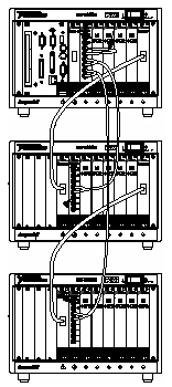
Figure 11. Illustration of multichassis synchronization that uses the NI PXI-6653 system timing and control module whereby the 10 MHz reference clock and triggers are distributed from a master chassis to all slave chassis, with NI MXI-4 controlling all slave chassis.
The purpose of NI-TClk synchronization is to have devices respond to triggers at the same time. The “same time” means on the same sample period and having very tight alignment of the sample clocks. NI-TClk synchronization is accomplished by having each device generate a trigger clock (TClk) that is derived from the sample clock. Triggers are synchronized to a TClk pulse. A device that receives a trigger from an external source or generates it internally will send the signal to all devices, including itself, on a falling edge of TClk. All devices react to the trigger on the following rising edge of TClk. The TClk frequency is much lower then the sample clock and the PXI 10 MHz reference clock to accommodate the NI PXI-1045 18-slot chassis, where the propagation delay from Slot 1 to Slot 18 may extend to several nanoseconds. If the application calls for multiple chassis where the propagation delay can be higher then normal interchassis delay, you can set the TClk frequency.
The issue of “instantaneous” data acquisition comes up; if a trigger condition is met and 10 digitizers are required to be triggered, the issue of latency arises due to the synchronization of the trigger to TClk. This issue is addressed with pretrigger and posttrigger samples on the device sample memory buffer. All NI-TClk supported devices are programmed to accommodate the overhead time that arises from synchronization of the trigger to the TClk. For example, 10 digitizers are programmed to acquire 10,000 samples simultaneously. The sample rate is 200 MS/s (sample period of 5 ns) from which the derived TClk frequency is programmed to be 5 MHz (sample period of 200 ns). This implies that the delay in acquisition resulting from TClk synchronization of the trigger could be as high as 40 samples. NI-TClk supported devices are programmed to automatically pad the memory buffer for the lag between the trigger event and the start of acquisition, and the NI-TClk driver software automatically adjusts the timestamps on all digitizers to reflect the start of acquisition with respect to the trigger event.
Overview of NI-TClk Operation with an Internal (PXI) Reference Clock or User-Supplied Reference Clock
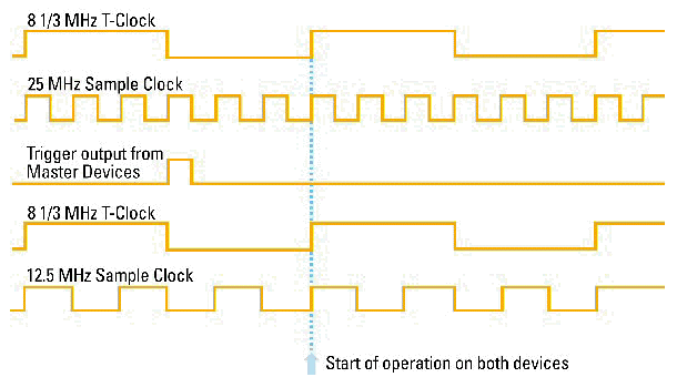
The devices are synchronized in the following manner. Refer to Figure 12 for the timing diagram that illustrates sample clock alignment and Figure 13 for trigger distribution and reception.
- Each device is programmed with a sample clock rate, and set to receive the TClk trigger.
- NI-TClk software automatically calculates the TClk frequency based on the sample clocks and number of devices involved, and TClks are generated on each device, derived from the sample clocks of the devices.
- The PXI 10 MHz reference clock (in PCI the onboard reference clock of one of the devices is used) is distributed to all devices to phase-lock the sample clocks on all devices.
- Each device sample clock is phase-locked to the 10 MHz reference clock but is not necessarily in phase with each other at this stage.
- A common clock signal called the Sync Pulse Clock is distributed through the PXI trigger bus (over the RTSI bus for PCI boards) to all devices whose frequency is similar to the reference clock frequency. Here the 10 MHz reference clock plays the role of the Sync Pulse Clock in addition to being the reference clock.
- A Sync Pulse is generated from one of the devices when the Sync Pulse Clock (10 MHz reference clock) is logically high through the PXI trigger bus (over the RTSI bus for PCI boards).
- Each device is initiated to look for the first rising edge of the Sync Pulse Clock upon receiving the Sync Pulse.
- When the first rising edge of the Sync Pulse Clock is detected, each device is programmed to measure the time between this edge and the first rising edge of the device TClk. The time between these two edges is measured on all devices.
- TClk measurements of all devices are compared to one reference TClk measurement (the NI-TClk driver software automatically selects one of the devices), and all device sample clocks and TClks are aligned automatically by adjusting the phase DAC outputs on all devices.
- With the sample clocks on all devices aligned, the trigger signal is distributed from the appointed master to all other devices through the TClk. The trigger signal is emitted with the falling edge of the master device TClk, and all devices are programmed to initiate generation or acquisition with the next rising edge of TClk. This signal is also distributed through the PXI trigger bus (over the RTSI bus for PCI boards). See Figure 13.
Two Properties of NI-TClk Synchronization are critical to the success of the method:
- The distribution of the Sync Pulse is critical to NI-TClk synchronization. The Sync Pulse must arrive at each device such that each device looks for the same rising edge of the Sync Clock Pulse in making the TClk measurement. The skew cannot exceed the period of the Sync Pulse Clock. This issue is easily resolved with the Sync Pulse Clock period being 100 ns. NI-TClk synchronization can easily extend from synchronization within one chassis to several dozen, as the standard delay per foot of 50 Ω cable is of the order of 2 ns.
- The accuracy of the sample clock alignment is as good as the skew of the Sync Pulse Clock (reference clock). In looking at Figure 12, you can see that the reference clock received on both devices is skewed. The TClk measurements on both devices assume that the Sync Pulse Clock is aligned on both devices; the difference between the two TClk measurements is used to shift the sample clocks to align them. As will be seen in the following section, two levels of performance can be achieved with current technology; out-of-the-box performance and calibrated performance.
Figure 12. Timing Diagram of Using TClk to Align Sample Clocks
Figure 13. Timing Diagram of Trigger Distribution Using NI-TClk
Overview of NI-TClk Operation with a User-Supplied External Sample Clock
In this scheme, NI-TClk synchronization will not align the sample clock on each device, because you are externally supplying the sample clock, bypassing the PLL circuitry. NI-TClk synchronization guarantees the start/stop trigger distribution such that each device starts and stops acquisition/generation on the same sample clock edge. NI-TClk does this by using the same method as mentioned above in using a derived TClk from the sample clock to distribute the trigger signals.
Here, the burden of accurate sample clock alignment is placed on the sample clock you supply. To ensure the best performance, supply a low-jitter sample clock (of the order of <1 psrms) for sample rates above 100 MS/s with equal length line cables from the clock source to each device in the system.
Refer to Figure 13 for an illustration of trigger distribution and reception.
- Each device is programmed to receive the TClk trigger and the external sample clock.
- NI-TClk automatically calculates the TClk frequency based on the sample clocks and number of devices involved. Then, TClk signals are generated on each device, derived from the device sample clock.
- The trigger signal is distributed from the appointed master to all other devices using NI-TClk; the trigger signal is emitted with the falling edge of the master TClk, and all devices are programmed to initiate generation or acquisition with the next rising edge of TClk. This signal is also distributed through the PXI trigger bus (over the RTSI bus for PCI boards). Refer to Figure 13 for an illustration.
Performance of NI-TClk Technology
Out-of-the-Box Performance
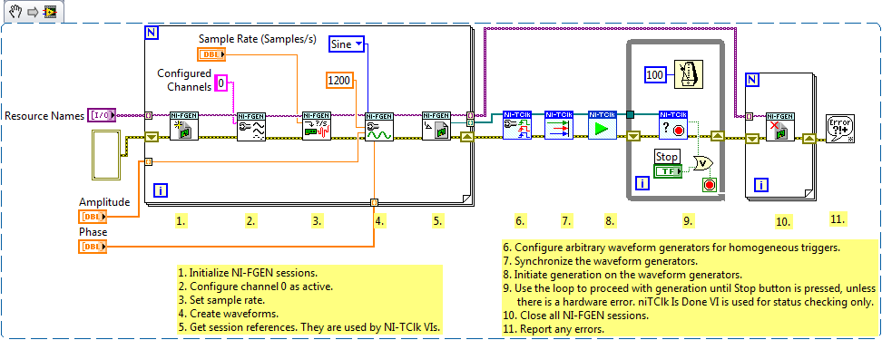
Robust synchronization of multiple devices can be achieved by simply inserting the devices into the PXI chassis and running the devices using NI-TClk software (refer to Figure 14 for an illustration). The key software components consist of three VIs/functions that require you to set no parameters.
Figure 14. LabVIEW Block Diagram Using NI-TClk Synchronization between Multiple FGEN Arbitrary Function Generators
NI-TClk synchronization can deliver synchronized devices with skews of up to 1 ns between each device in a NI PXI-1042 chassis. The typical skews observed range from 200 to 500 ps. The channel-to-channel jitter between devices is dependent on the intrinsic system jitter of the device. For example, the NI PXI-5421 100 MS/s 16-bit AWG has a total system jitter of 2 psrms. NI-TClk synchronized PXI-5421 devices exhibit typical channel-to-channel jitter of under 5 psrms. With the NI PXI-5122 100 MS/s 14-bit digitizer, the channel-to-channel jitter is typically under 10 psrms.
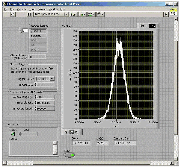
Figure 15. Out-of-the-Box Performance of NI-TClk Synchronization of Two 100 MS/s Digitizers
The LabVIEW front panel in Figure 15 is a measurement of the skew between two NI PXI-5122 devices in an NI PXI-1042 chassis. The skew is approximately 523 ps in this measurement setup. Each digitizer is set to sample the same 5 MHz square waveform at 100 MS/s. The signal is split and fed into each digitizer with equal length cables. The channel-to-channel jitter is approximately 6 psrms. The statistics are compiled from 49,998 zero crossings of the square waveform. The Gaussian distribution of the histogram reflects that the jitter stems from random noise rather any source of deterministic noise sources in the system.
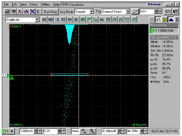
Figure 16. Channel-to-Channel Jitter Measurements of NI-TClk Synchronized PXI-5421 Arbitrary Waveform Generators
Figure 16 is a measurement of the channel-to-channel jitter of two NI-TClk synchronized PXI-5421 arbitrary waveform generators. Each device was programmed to generate a 10 MHz square waveform at 100 MS/s. The measurement was performed on a Tektronix high-performance jitter measurement Communications Signal Analyzer (CSA) 8200 platform with the 80E04 TDR module. The histogram data in Figure 16 reflects a channel-to-channel jitter of under 3 psrms. The median of the histogram reported is not the skew between the channels; it is the delay from the trigger of the zero crossing of the square waveform to the next rising edge of the measured square waveform (i.e. one channel is used to trigger the measurement of the zero crossing of the second channel). The measurements are compiled in a histogram which reflects the channel-to-channel jitter.
Calibrated NI-TClk Synchronization
As mentioned previously, the typical skews can range from 200 ps to 500 ps. This skew may not be satisfactory for some applications where the phase accuracy between channels requires a higher level of performance. In this case, manual calibration is required. Manual calibration can lower skews to less than 30 ps between devices. In Figure 17, a LabVIEW front panel illustrates the skew between the NI PXI-5122 100 MS/s digitizer and the NI PXI-5124 200 MS/s digitizer. The skew was found to be of the order of 15 ps with channel-to-channel jitter of 12 psrms. The statistics are compiled from 10,000 zero crossings of the square waveform.
Figure 17. Calibrated NI-TClk Synchronization of Two Digitizers – NI PXI-5122 at 100 MS/s and an NI PXI-5124 at 200 MS/s – Typical Skew on the Order of 15 psrms with Channel-to-Channel Jitter of 12 psrms
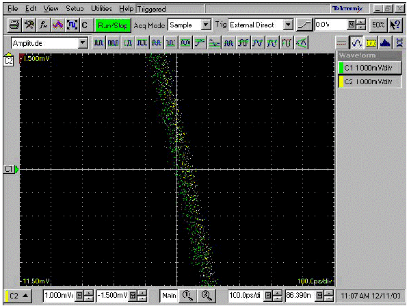 Figure 18. Magnified View of the Falling Edge of 10 MHz Square Waveform from Manually Calibrated NI-TClk Synchronized NI PXI-5421 Arbitrary Waveform Generators – Skew on the Order of 20 ps
Figure 18 is a measurement of the skew between two manually calibrated NI-TClk synchronized PXI-5421 arbitrary waveform generators using the CSA 8200. Notice that the skew is of the order of 20 ps. The waveform generated from the two devices is a 10 MHz square waveform.
Manual calibration involves the adjustment of the sample clock on each device with respect to each other using the phase adjustment DACs in the PLL circuitry (refer to Figure 8). In synchronizing two arbitrary waveform generators, for example, the synchronized outputs can be viewed on a high-speed oscilloscope and the sample clock on one AWG can be moved relative to the other, using the phase-adjustment DAC. Through this manual process, the skew between multiple arbitrary waveform generators can be minimized from hundreds of picoseconds to under 30 ps.
In synchronizing two digitizers, a low-phase noise signal is fed into each digitizer with equal length line cables. The skew can be measured in software, and the sample clock of one digitizer can be adjusted relative to the other to minimize the skew. The same methods are used in synchronizing digital waveform generator/analyzers.
The sample clock adjustment can be achieved with high resolution. On the 100 MS/s devices, such as the PXI-5122, PXI-5421, and PXI-6552, the sample clock delay adjustment resolution is 10 ps and can be adjusted to ±1 sample clock period of 10 ns. On the 200 MS/s devices, such as the PXI-5422 and the PXI-5124, the adjustment resolution is 5 ps and can be adjusted to ±1 sample clock period of 5 ns. Thus, the skew between devices can be manually calibrated with high accuracy.

