Researchers from RMIT University used a non-toxic liquid gallium metal alloy to synthesize two-dimensional sheets of materials used in electronic components quickly, cheaply and without special equipment.
The beauty of the technique is in its simplicity, according to University of Auckland computational physicist Nicola Gaston, who specializes in gallium and two-dimensional structures.
“They’re exploiting the properties of gallium in a very clever way,” she said.

Thin layers of metal oxides — compounds containing metal atoms bound to oxygen — are widely used in electronics. The touchscreen on your smartphone, for instance, uses metal oxides, as do transistors, the building blocks of modern electronics technologies.
The thinner the metal oxide layer, the faster and more energy efficient the electronic component is.
Making these ultra-thin layers today usually involves evaporating metal in a low-pressure chamber and allowing it to condense on a surface, producing layers more than 10 atoms thick.
But not only does this technique require special equipment, the layers aren’t smooth, study co-author Professor Kourosh Kalantar-Zadeh said.
When the evaporated metal oxide starts to condense on a surface, it forms “islands” — a bit like steam condensing as droplets on a window — that grow and join up to produce a single layer, he said.
When electrons are blocked, efficiency drops.
The new technique creates smooth metal oxide layers without boundaries, so electrons can move unimpeded.
The layers are only two or three atoms thick, and they don’t require special equipment to produce — just a stovetop and a couple of ingredients.
To produce a metal oxide commonly used as an electrical insulator — called hafnium dioxide — the researchers dissolved powdered hafnium in a gallium alloy over a low heat.
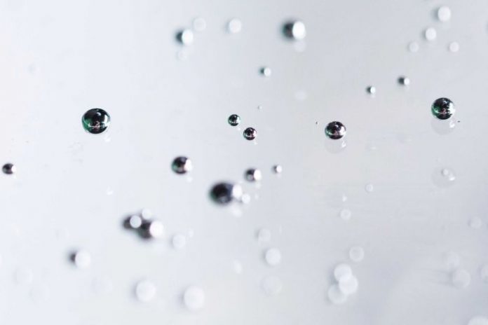
When dropped on a surface as a blob, the hafnium atoms make their way to the outer layer of the metal concoction where they react with oxygen in the air, producing hafnium dioxide.
Removing this metal oxide layer is “surprisingly easy”, according to materials chemist and study co-author Torben Daeneke.
Simply touching the surface of the blob, or letting it roll across a surface, peels the metal oxide away from the liquid below in a uniform sheet, with no boundaries or holes.
Any metal that’s more reactive than the gallium will do the trick. “We think the technique could be applied to a third of the periodic table,” Dr. Daeneke said.
The future is tiny
Agustin Schiffrin, an experimental condensed matter physicist at Monash University, says the work is “very relevant” to the future of electronics.
Transistors comprise three layers of materials: an active material (semiconductor) that can or cannot conduct electricity, a second material (metal) that controls the electrical conductivity of the first active material, and an insulator between the two.
At the moment, silicon dioxide is the insulator of choice for transistors. But it loses some of its insulating properties when it’s used as a thin layer, Dr. Schiffrin said.
“Hafnium dioxide is a very efficient insulator. Importantly, it remains highly insulating even when it becomes very thin.
“The fact that you can have a material that is at the same time efficiently insulating and atomically thin means you could arguably make a transistor with a thickness of only three atomic layers.”
Source: ABC News


