Solar panels, also known as photovoltaics, rely on semiconductor devices, or solar cells, to convert energy from the sun into electricity.
To generate electricity, solar cells need an electric field to separate positive charges from negative charges. To get into this field, manufacturers typically dope the solar cell with chemicals so that one layer of the device bears a positive charge and another layer has a negative charge. This multi-layered design ensures that electrons flow from the negative side of a device to the positive side—a key factor in device stability and performance. But chemical doping and layered synthesis also add extra costly steps in solar cell manufacturing.
Now, a team of researchers led by scientists at DOE’s Lawrence Berkeley National Laboratory (Berkeley Lab), in collaboration with UC Berkeley, have demonstrated a unique workaround that offers a simpler approach to solar cell manufacturing: A crystalline solar material with a built-in electric field—a property enabled by what scientists call “ferroelectricity.
The new ferroelectric material—which is grown in the lab from cesium germanium tribromide (CsGeBr3 or CGB)—opens the door to an easier approach to making solar cell devices. Unlike conventional solar materials, CGB crystals are inherently polarized, where one side of the crystal builds up positive charges and the other side builds up negative charges, with no doping required.
In addition to being ferroelectric, CGB is also a lead-free “halide perovskite,” an emerging class of solar materials that have intrigued researchers for their affordability and ease of synthesis compared to silicon. But many of the best-performing halide perovskites naturally contain the element lead. According to other researchers lead remnants from perovskite solar material production and disposal could contaminate the environment and present public health concerns. For these reasons, researchers have sought new halide perovskite formulations that eschew lead without compromising performance.
“If you can imagine a lead-free solar material that not only harvests energy from the sun but also has the added bonus of having a natural, spontaneously formed electric field—the possibilities across the solar energy and electronics industries are pretty exciting,” said co-senior author Peidong Yang, a leading nanomaterials expert known for his pioneering work in one-dimensional semiconducting nanowires for novel solar cell technologies and artificial photosynthesis. He is a senior faculty scientist in Berkeley Lab’s Materials Sciences Division and a professor of chemistry and materials science and engineering at UC Berkeley.
CGB could also advance a new generation of switching devices, sensors, and super-stable memories that respond to light said co-senior author Ramamoorthy Ramesh, who held titles of senior faculty scientist in Berkeley Lab’s Materials Sciences Division and professor of materials science and engineering at UC Berkeley at the time of the study and is now vice president of research at Rice University.
Perovskite solar films are typically made using low-cost solution-coating methods, such as spin coating or inkjet printing. And unlike silicon, which requires a processing temperature of about 2,732 degrees Fahrenheit to manufacture into a solar device, perovskites are easily processed from solution at room temperature to around 300 degrees Fahrenheit—and for manufacturers, these lower processing temperatures would dramatically reduce energy costs.
But despite their potential boost to the solar energy sector, perovskite solar materials won’t be market-ready until researchers overcome long-standing challenges in product synthesis and stability and material sustainability.
Pinning down the perfect ferroelectric perovskite
Perovskites crystallize from three different elements, and each perovskite crystal is delineated by the chemical formula ABX3
Most perovskite solar materials are not ferroelectric because their crystalline atomic structure is symmetrical, like a snowflake. In the past couple of decades, renewable energy researchers like Ramesh and Yang have been on the hunt for exotic perovskites with ferroelectric potential—specifically, asymmetrical perovskites.
A few years ago, first author Ye Zhang, who was a UC Berkeley graduate student researcher in Yang’s lab at the time, wondered how she could make a lead-free ferroelectric perovskite. She theorized that placing a germanium atom in the center of a perovskite would distort its crystallinity just enough to engender ferroelectricity. On top of that, a germanium-based perovskite would free the material of lead. (Zhang is now a postdoctoral researcher at Northwestern University.)
But even though Zhang had honed in on germanium, there were still uncertainties. After all, conjuring up the best lead-free, ferroelectric perovskite formula is like finding a needle in a haystack. There are thousands of possible formulations.
So Yang, Zhang, and the team partnered with Sinéad Griffin, a staff scientist in Berkeley Lab’s Molecular Foundry and Materials Sciences Division who specializes in the design of new materials for a variety of applications, including quantum computing and microelectronics.
With support from the Materials Project, Griffin used supercomputers at the National Energy Research Scientific Computing Center (NERSC) to perform advanced theoretical calculations based on a method known as density-functional theory.
Through these calculations, which take atomic structure and chemical species as input and can predict properties such as the electronic structure and ferroelectricity, Griffin and her team zeroed in on CGB, the only all-inorganic perovskite that checked off all the boxes on the researchers’ ferroelectric perovskite wish list: Is it asymmetrical? Yes, its atomic structure looks like a rhombohedran, rectangle’s crooked cousin. Is it really a perovskite? Yes, its chemical formula—CeGeBr3 –matches the perovskite’s telltale structure of ABX3.
The researchers theorized that the asymmetric placement of germanium in the center of the crystal would create a potential that, like an electric field, separates positive electrons from negative electrons to produce electricity. But were they right?
Measuring CGB’s ferroelectric potential
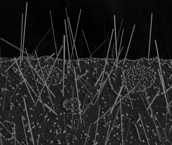
To find out, Zhang grew tiny nanowires (100 to 1,000 nanometers in diameter) and nanoplates (around 200 to 600 nanometers thick and 10 microns wide) of single-crystalline CGB with exceptional control and precision.
“My lab has been trying to figure out how to replace lead with less toxic materials for many years,” said Yang. “Ye developed an amazing technique to grow single-crystal germanium halide perovskites —and it’s a beautiful platform for studying ferroelectricity.”
X-ray experiments at the Advanced Light Source revealed CGB’s asymmetrical crystalline structure, a signal of ferroelectricity. Electron microscopy experiments led by Xiaoqing Pan at UC Irvine uncovered more evidence of CGB’s ferroelectricity: a “displaced” atomic structure offset by the germanium center.
Meanwhile, electrical measurement experiments carried out in the Ramesh lab by Zhang and Eric Parsonnet, a UC Berkeley physics graduate student researcher and co-author on the study, revealed a switchable polarity in CGB, satisfying yet another requirement for ferroelectricity.
But a final experiment—photoconductivity measurements in Yang’s UC Berkeley lab—yielded a delightful result and a surprise. The researchers found that CGB’s light absorption is tunable—spanning the spectrum of visible to ultraviolet light (1.6 to 3 electron volts), an ideal range for coaxing high energy conversion efficiencies in a solar cell, Yang said. Such tunability is rarely found in traditional ferroelectrics, he noted.
Yang says there is still more work to be done before the CGB material can make its debut in a commercial solar device, but he’s excited by their results so far. “This ferroelectric perovskite material, which is essentially a salt, is surprisingly versatile,” he said. “We look forward to testing its true potential in a real photovoltaic device.”


