

Courtesy: Lam Research
Line edge roughness (LER) is a variation in the width of a lithographic pattern along one edge of a structure inside a chip. Line edge roughness can be a critical variation source and defect mechanism in advanced logic and memory devices, and can lead to poor device performance or even device failure [1~3]. Deposition-etch cycling is an effective technique to reduce line edge roughness. In this study, we demonstrate how virtual fabrication can provide guidance on how to perform deposition/etch cycling in order to reduce LER.
A typical line and via array pattern with a pitch of 40 nm was established as a test structure in the virtual fabrication software. Pattern critical dimensions (CD) and LER amplitude and correlation length (measures of line edge roughness) were then explored under different experimental conditions.


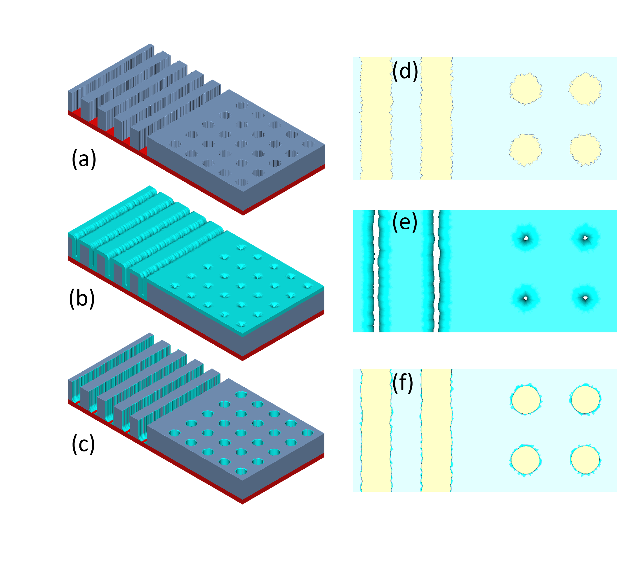
A deposition/etch cycling process was applied in a virtual model to improve the line edge roughness (LER) and critical dimension uniformity (CDU) of the pattern (Figure 1). Virtual metrology was used to measure LER standard deviation (LERSTD), LER correlation length (C) and Via CD range (VCDR) to evaluate the impact of the selected process changes on LER and CDU improvement.
We ran 1,500 virtual experiments using the incoming pattern CD, LER amplitude (A), LER correlation length (C), etch/deposition amount (THK), and number of deposition/etch cycles (NC) as experimental variables. Part of the results of our experiment are shown in Figure 2.
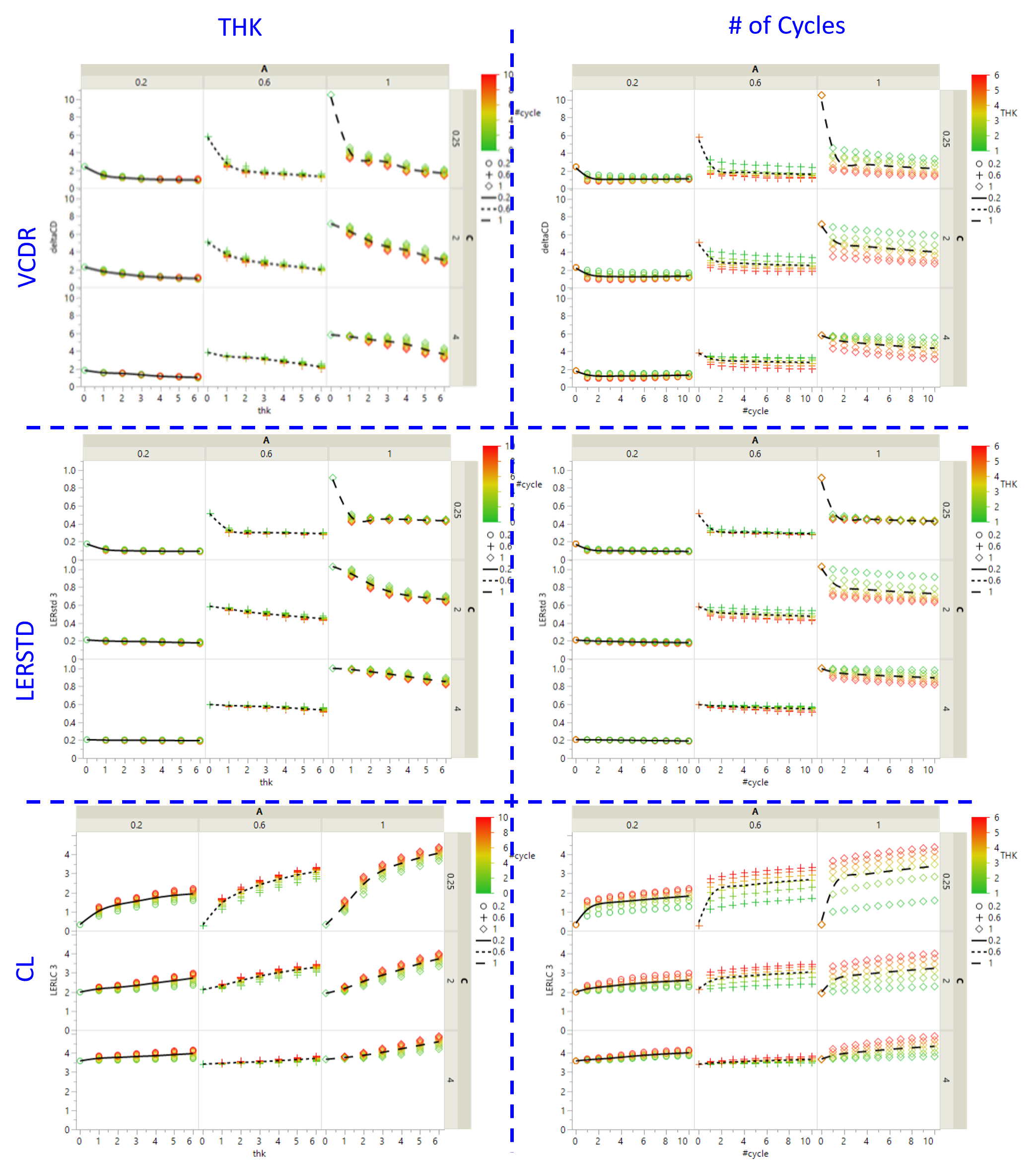
Figure 2 shows the trend in the Via CD ranges (VCDR), LER standard deviation (LERSTD), and LER correlation length (C) values with respect to the number of deposition / etch cycles (bottom axis) at different LER A and LER C conditions (top and right axis). Our goal is to minimize VCDR, LERSTD and CL values at the lowest number of deposition / etch cycles. We can draw 3 conclusions from Figure 2.
1) Most of the improvement to LER/VCDR occurs in the first deposition/etch cycle.
2) An increase in the deposition amount (THK, shown in color on Figure 2) has a greater impact on the LER/VCDR improvement than an increase in the number of deposition/etch cycles.
3) The LER correlation length (C) becomes larger after a deposition/etch cycle, but the LER/VCDR improvement is not obvious when the LER correlation length (C) increases.
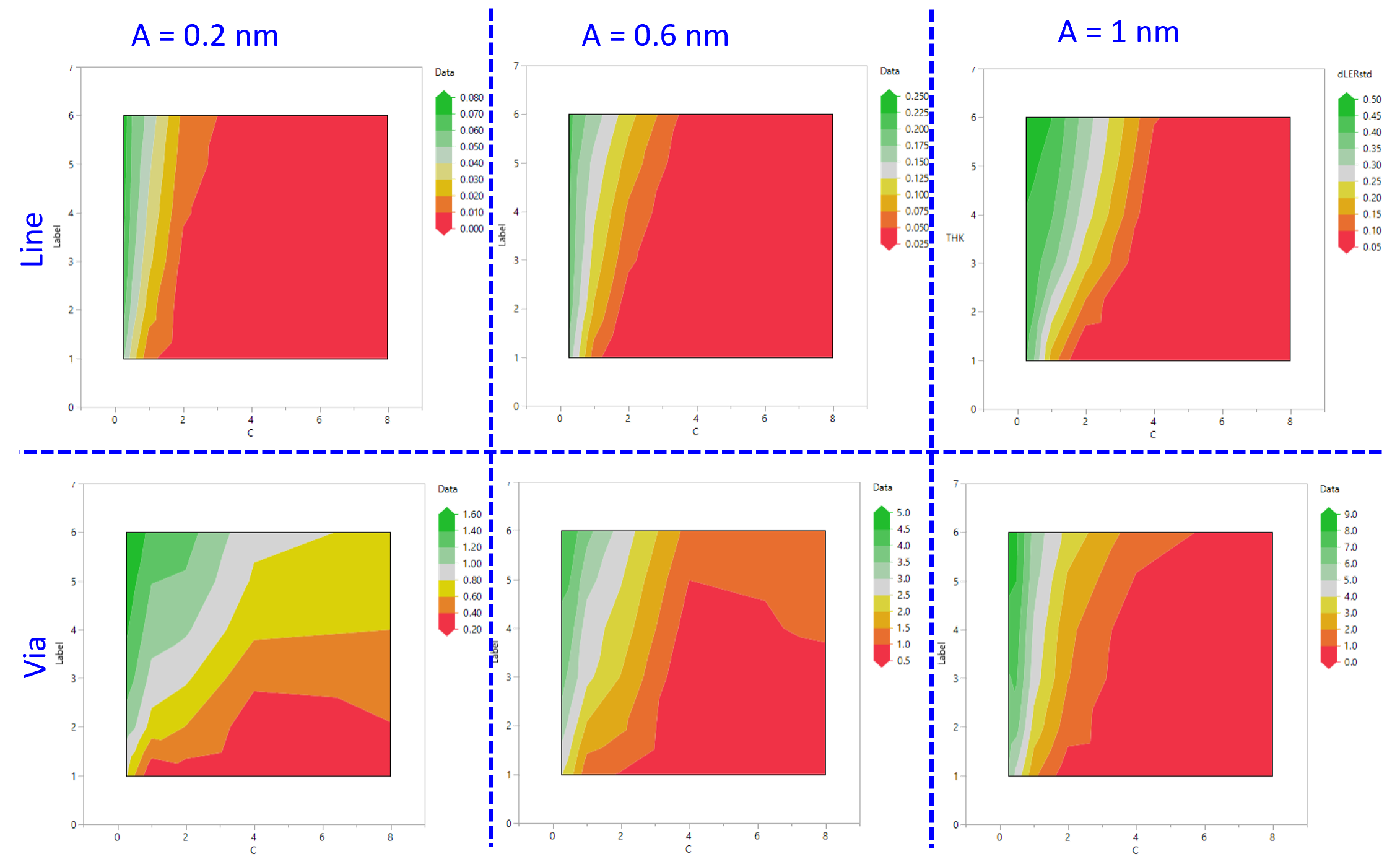
As we mentioned earlier, most of the LER improvement happened in the first deposition/etch cycle, with the remaining deposition/etch cycles producing a much smaller improvement. Contour plots displaying the LER/VCDR improvement on the 1st cycle was fitted and illustrated in Figure 3. From Figure 3, we can draw 2 conclusions:
1). Although less improvement was noticed with a larger incoming LER correlation length (C), improvement still occurred at the via patterns if a thicker film was used during the deposition portion of the cycle when there was a larger LER correlation length (LER C) and lower LER amplitude (LER A).
2). LER/VCDR can be improved using a relatively thicker deposition film at larger incoming LER C conditions.
In this study, a deposition/etch cycling process was simulated to improve LER and CDU performance at advanced nodes by virtual fabrication. The results indicate that most of the LER/VCDR improvement seen during deposition/etch cycling processes occurred during the first deposition/etch cycle. The deposition/etch cycling process is very effective in reducing high frequency noise (when there is a smaller LER correlation length). LER improvements are larger at the via patterns than at the line patterns when a thicker film is deposited, exhibiting as larger LER correlation length values and lower LER amplitude. These results provide quantitative guidance on the optimal selection of deposition/etch amounts and the number of cycles needed, to both reduce LER and lower defects and variability in the production of advanced semiconductor devices.