

Courtesy : LAM RESEARCH
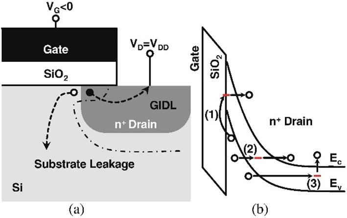
Gate-induced drain leakage (GIDL) presents a major challenge in scaling DRAM technology.
DRAM serves as the backbone of modern computing, enabling devices ranging from smartphones to high-performance servers. As the demand accelerates for higher density and lower power consumption in memory devices, innovation in reducing DRAM leakage currents and enhancing performance becomes essential. One significant challenge in scaling DRAM technology is GIDL, a primary source of standby charge loss. This article explores how a DWMG structure in DRAM buried word-line (BWL) can mitigate GIDL. By leveraging a full-scale process integration model that supports electrical analysis, we demonstrate how this approach reduces leakage current while maintaining robust device performance.


The Challenge of GIDL in Modern DRAM
GIDL is primarily caused by band-to-band tunneling (BTBT) at the drain junction under high electric field conditions. This phenomenon not only increases off-state leakage currents but also degrades memory state retention time in DRAM cells, particularly as feature sizes shrink below 20 nm.1
Factors such as thinner gate oxides and higher doping concentrations exacerbate GIDL, creating a synergistic effect that makes it a critical problem in designing low-power, high-density DRAM.2
The Solution
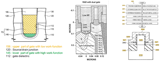
The introduction of a dual work-function metal gate structure provides a compelling solution to this challenge. By segmenting the buried word-line gate into regions with distinct work functions, the electric field along the channel is precisely controlled. Examples of some dual work-function metal gate structures are shown in Figure 2.
This structure suppresses BTBT generation, thereby reducing GIDL without compromising drive current or threshold voltage (Vt). As a result, this design is well-suited for advanced DRAM nodes.4,5
DWMG Alignment with Industry Trends
The DWMG approach aligns with broader semiconductor trends emphasizing advanced gate designs and channel engineering. Our study applies this innovation to DRAM technology, addressing GIDL challenges while preserving key performance metrics. Similar methods have been successfully implemented in FinFETs6 and tunnel FETs7 to reduce leakage and improve subthreshold slopes.
Leveraging Process Integration Modeling for Insights
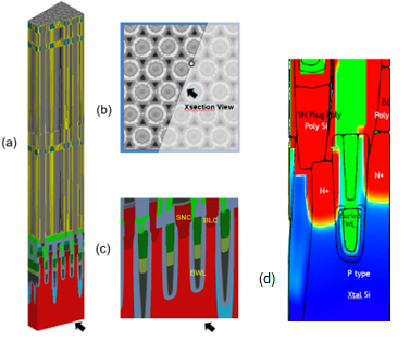
Our process integration modeling platform (SEMulator3D) with built-in electrical analysis capabilities played a pivotal role in evaluating the DWMG design. This tool allowed us to:
- Simulate the full process flow of a DRAM cell array, from active area formation to capacitor integration (Figure 3a).
- Focus on the BWL transistor by extracting and refining a specific transistor for electrical characterization (Figure 3b–d).
- Analyze the interactions between process parameters—such as gate work-function, oxide thickness, and doping profiles—and their impact on electrical performance.
This simulation framework provided a holistic view of integration challenges and revealed the effectiveness of DWMG in reducing current leakage.
DWMG Design and Simulation Results
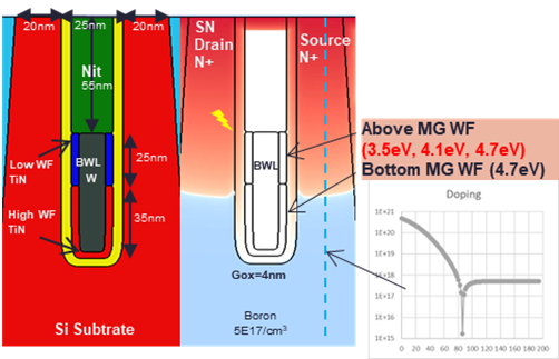
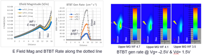
The DWMG structure is realized by splitting the gate into upper and lower regions with distinct work functions in the upper region’s metal gate of 3.5eV, 4.1eV, and 4.7eV (Figure 4). The device simulation considers the models of doping/field-dependent mobility, Shockley-Read-Hall (SRH) generation/recombination, and trap-assisted band-to-band tunneling effects.
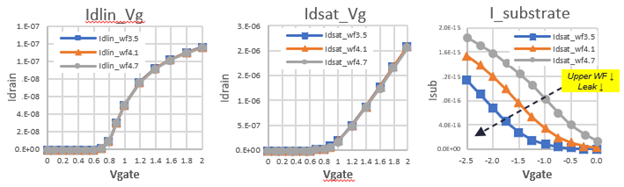
The drift-diffusion equation is solved to obtain Idrain vs. Vgate curves, both in the linear and saturation regimes. The substrate current is measured (virtually) to determine the GIDL leakage amount.
Key results include the following:
- Leakage reduction (Figure 5): The low and high work-function regions, in the upper gate and lower gate, respectively, create a more relaxed electric field distribution than the same work-function without the DWMG, which suppresses BTBT at the drain junction and in turn reduces leakage current.
- Preserved device performance (Figure 6): Despite the GIDL reduction (I_subtrate), critical IV characteristics in both linear (Idlin_Vg) and saturation (Idsat_Vg) regimes remain intact when using the DWMG, ensuring reliable operation during read and write cycles.
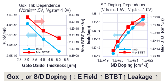
- Process dependency (Figure 7): Gate oxide thickness and doping concentration significantly influence performance. For instance, thinner oxides improve field control but increase BTBT risk due to the reduced barrier width. Similarly, higher doping improves modulation capabilities but exacerbates BTBT by increasing the electric field intensity, which accelerates tunneling processes.
Advantages of Combining Device Electrical Analysis with Process Integration Modeling
Performing device electrical analysis during process integration modeling can enable the following types of advanced analyses that identify design-technology trade-offs:
- Electrical pathfinding: This type of analysis can be used to rapidly explore combinations of gate work-functions, oxide thicknesses, and doping profiles to pinpoint optimal designs. This approach has the potential to minimize the cost and time of physical experiments while reducing risks associated with late-stage failures.
- Variability analysis: Statistical simulations can identify the impact of process variations—such as gate oxide non-uniformity and doping fluctuations—on GIDL and IV characteristics. This type of analysis highlights critical design margins and has the potential to provide feedback on process optimization (such as active area formation) from very early process development stages.
The Future of DWMG and DRAM
The dual work-function metal gate (DWMG) is a robust, scalable solution for mitigating GIDL in DRAM technology. By optimizing the electric field distribution, this design effectively reduces leakage currents while maintaining critical IV performance. Process integration modeling combined with electrical analysis capabilities is instrumental in demonstrating the ability to reduce leakage current using DWMG, offering a comprehensive framework for addressing design and integration challenges.
Future research efforts could include:
- Integrating DWMG designs with high-k dielectrics or advanced junction engineering to further enhance leakage control.
- Assessing the impact of scaling trends, such as smaller metal pitches and EUV lithography, on DWMG performance.
- Developing predictive models for variability in advanced DRAM nodes.