The accelerating deployment of electrical and electronic systems for mobile, automotive, and the Internet of Things (IoT), combined with narrowing time-to-market windows, has led to a need for more rapid, lower cost tests of the ICs that support them.
Achieving these goals requires automated IC test platforms with greater flexibility and modularity, as well as reduced component count to save on both cost and space.
To meet these requirements, designers are shifting from classic analog controllers to digital control loops that are readily programmable to achieve loop stability. Although the digital controller removes resistors, capacitors, and switches, the resolution and accuracy of the analog-to-digital converter (ADC) and digital-to-analog converter (DAC) greatly influence the overall accuracy of the digital control loop architecture.
This article briefly discusses the advantages of a digital control loop. It then discusses implementation challenges, such as timing and converter noise error sources, and their management through careful attention to an ADC’s throughput rate and signal-to-noise ratio (SNR), and the DAC’s settling time and noise spectral density specifications.
It then introduces Analog Devices’ AD4630-24, a 24-bit successive approximation register (SAR) ADC, and Analog Devices’ AD5791 voltage output DAC. These two devices, when combined, can form the basis of a highly accurate and flexible digital controller for precision instrumentation measurements.
Digital control loops
In engineering systems, controllers ensure satisfactory transient and steady-state behavior. An analog controller implementation has analog inputs and outputs where signals exist along a continuous time interval, with values in a continuous amplitude range. A sensor measures the controlled variable and compares its behavior to a reference signal. The test control action uses an error signal, which is the difference between the reference and the actual values (Figure 1).
 Figure 1: An analog system motor controller uses various amplifiers (U1-U5) and a collection of predetermined resistor and capacitor values. (Image source: Quora)
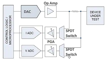
Intuitively, controllers with continuous system analog output would seem superior to digital controllers with their sampled output values (Figure 2).
 Figure 2: A measurement system using a digital controller configuration with a DAC, two ADCs, analog amplifiers, and switches. (Image source: Bonnie Baker)
Logic would point to the control variables or outputs in an analog controller that change continuously to achieve better control than the measurements that change periodically in digital structures.
This deduction is valid. Assuming all other digital and analog control factors are identical, analog control is superior to digital control. So, why change the classic controller from analog to digital? The five reasons are accuracy, implementation errors, flexibility, speed, and cost.
Accuracy: The digital representation of analog signals is in terms of zeros and ones, with up to 32 bits typically used to represent a single analog value (Figure 2). These conversions create a small digital quantization error that needs to be addressed. Analog signals, on the other hand, have power-supply drifts and external noise that degrade the analog signal. These analog temperature and time-related drifts are difficult and expensive to control, whereas the effects of aging and temperature on digital controllers are negligible.
Implementation errors: Implementation errors are negligible in the digital controller. This is because the digital processing of control signals uses stored numerical values for addition and multiplication functions, rather than analog components with their temperature drift errors, and the unreliable out-of-box accuracy of resistors, capacitors, and inductors. Also, a digital controller’s time-constant settings are easily modified in software, whereas an analog controller has a fixed number of available time constants. The digital controller’s changes can be made on-the-fly, allowing the instrument to adapt to various load conditions and improve overall test efficiency.
Flexibility: Analog controllers present flexibility difficulties. After the hardware design is complete, modifications to the pc board are time-consuming and costly. With a digital controller, modifications are easy to implement—down to a total code replacement. Additionally, there are no constraints on the digital controller’s form or structure, and complex controller structures involving extra arithmetic options are easily realizable.
Speed: Computing performance continues to increase exponentially. This increase makes it possible to sample and manage signals at very high rates, and the interval between samples continues to be smaller and smaller. A modern digital controller’s performance is equivalent to a continuous analog monitoring system.
Cost: Thanks to advances in semiconductor manufacturing, the cost of ICs continues to fall, making digital controllers more economical—even for small, low-cost applications.
Analog implementation challenges for digital controllers
The ADC and DAC are at the boundary of the analog and digital domains, both of which have various electrical characteristics. The trick is to discover the complementary specifications between the two devices so they can coexist in the same system. From a system throughput perspective, it is crucial to nail down the speed and noise characteristics of the overall transfer.
The ADC and DAC timing estimates
There is usually a clear definition of the ADC’s throughput rate in mega samples-per-second (MSPS) or kilo samples-per-second (kSPS). The throughput time in frequency Hertz is the inverse of the throughput rate in seconds. The throughput time is the time required for the converter to sample, acquire, digitize, and prepare for the subsequent conversion. This time is also the minimum conversion time in a continuous conversion application. The specification units define the conversion speed of a complete output word. For instance, if the ADC has a digital serial output pin and the converter has 24-bits, the entire 24-bit conversion of the analog input is transmitted before the start of another conversion (Figure 3).
 Figure 3: The ADC timing diagram illustrates the number of digital codes the converter accepts. (Image source: Analog Devices)
An ADC with a 2 MSPS specification outputs a complete word every 500 nanoseconds (ns). Unfortunately, this single conversion sample does not paint a complete picture of an analog input signal. According to the Nyquist Theorem, the ADC must produce a minimum of two samples to enable the generation of the analog input signal. At a minimum, to meet the Nyquist Theorem, this process now requires two times 500 ns or 1 microsecond (µs) of time. This is a minimum number of samples to create a skeleton of the analog signal. Four or eight samples are preferable to recreate an analog signal digitally.
Moving to the DAC specifications, the DAC’s output voltage settling time is the amount of time it takes for the output voltage to settle to a specified level for a specified change in the voltage (Figure 4).
 Figure 4: A DAC exhibits a settling time error that captures the time required to reach the final value. The worst-case settling time error typically occurs when the output goes between the 100 000 and 011 111 … input codes. (Image source: Analog Devices)
Using Figure 4 as an example DAC, the worst-case settling time is less than 1 µs. The mathematical inverse of this value equals 1 MHz, which is also equal to 1 MSPS. To fit into the Nyquist criteria, the DAC must produce two output samples requiring two times 1 µs of time, or 2 µs, and as with the ADC, the more samples, the better.
Now, the final story about the Nyquist Theorem. According to the theorem, the reproduction of a signal requires a minimum of two samples. In this scenario, the theorem only identifies the signal frequency. This is where the theorem needs the application of common sense. The higher sample sizes take longer to collect, but they produce a more reliable signal reconstruction.
The ADC and DAC frequency noise estimates
The definition of noise requires understanding actual converter resolution and root-mean-square (rms) noise. The claim of converter resolution, such as 24-bit, 20-bit, or 1 ppm, describes the number of ADC or DAC outputs or inputs. For instance, a 24-bit ADC generates twenty-four output codes per conversion, and a 20-bit DAC collects twenty digital input values for one conversion. But with these values, there is no definition of the converter’s frequency accuracy.
The definition of a converter’s accuracy relies on noise specifications such as SNR or rms noise. An ADC specification for noise across the output frequency range is a typical decibel (dB) SNR value. SNR is calculated using Equation 1:
 Equation 1
The ADC or DAC datasheet defines the device’s output range. Noise is the cumulative root-sum square (RSS) across the frequency band of the converter.
The rms resolution is calculated using Equation 2:
 Equation 2
For an ADC with an SNR of 105.7 dB, the rms resolution is 17.6 bits, meaning the converter can handle accuracy reliably to this level. The DAC noise specification is usually a spectral noise density value, making it easy to quickly convert the DAC’s actual rms resolution. The output noise of the DAC is calculated using Equation 3:
 Equation 3
For instance, if a 20-bit DAC has a spectral noise density of 7.5 nanovolts/√Hz (nV/√Hz) and a bandwidth of 500 kilohertz (kHz), the DACNoise equals 5.3 µV (rms). From this value, the DAC’s rms resolution with a 5-volt output range equals 19.8 bits.
Digital controller and precision instrumentation
An example digital controller device-testing system for mobile, automotive, and IoT test circuits has nine devices plus one discrete resistor (Figure 5). The devices in this circuit are a microprocessor, ADC, DAC, driver amplifier, gain-adjustable instrumentation amplifier, and Analog Devices’ ADG1236 SPDT switch. The microprocessor manages the digital interfaces and data between the ADC and DAC, such as the Analog Devices AD4630-24 and the AD5791, respectively.
 Figure 5: A digital controller uses a microprocessor to manage the data to and from the ADC and DAC. The DAC requires a gained output driver amplifier, and the ADC requires an amplifier system to attenuate the signal. (Image source: Analog Devices)
The AD4630-24 is a 2 MSPS, 24-bit ±0.9 ppm integral non-linearity (INL) ADC with an SNR of 105.7 dB, which produces 17.6 bits (rms). With a 2 MSPS conversion speed, this ADC requires a minimum of four output samples to create analog signals. The INL represents the converter’s DC accuracy.
The AD5791 is a 20-bit ±1 LSB, INL 1 µs settling time 7.5 nV/√Hz spectral density DAC, ultimately creating 19.8 bits (rms). This DAC, at a speed of 1 MSPS, requires 4 µs to generate analog signals accurately.
The converters in this system also require operational amplifier (op amp) interfaces to manage output drive and analog gain. In Figure 5, the Analog Devices AD8675 is a 10 MHz, 2.8 nV/√Hz rail-to-rail output op amp. This amplifier’s noise brings the DAC system’s bits down to 19.1 (rms). However, the 10 MHz amplifier bandwidth surpasses the DAC’s bandwidth.
The Analog Devices LTC6373 fully differential, programmable-gain instrumentation amplifier provides gain and a degree of isolation. If the DAC stage implements a gain of 4 volts per volt (V/V), one of the gain options of the LTC6373 is 0.25 V/V which brings the signal back to the original value. The LTC6373’s digital gain levels’ flexibility contributes to the digital controller’s on-the-fly characteristics.
Conclusion
The time-to-market pressure and the cost of supporting the rapidly evolving design requirements of mobile, automotive, and IoT electronic test systems have seen a shift from classic analog controllers to digital control loops. These loops provide higher accuracy and flexibility and lower cost but require careful attention to the choice of ADC and DAC.
As shown, by pairing the Analog Devices AD4630-24 24-bit SAR ADC with the Analog Devices AD5791 20-bit voltage output DAC, it’s possible to create a highly accurate and flexible digital controller for precision instrumentation measurements.
Authored Article by: Bonnie Baker, Digi-Key


