

 uses electrical measurements to identify common manufacturing defects that occur in printed circuit board assemblies during their manufacturing process.)
Key takeaways:
- In-circuit tests identify a wide range of common manufacturing defects in printed circuit board assemblies (PCBAs).
- Keysight’s in-circuit test systems have boosted test throughputs, reduced labor-intensive test tasks, and saved costs for several automotive and general electronics manufacturers.
- Complementary techniques like boundary scans and vectorless tests are often used with in-circuit tests to expand overall test coverage.
The overall quality and operational reliability of any electronic device, be it a safety-critical defense weapon or a life-saving medical device, largely depends on the quality and reliability of the printed circuit board assemblies inside it.
The complexity of these assemblies and their manufacturing processes require several strategies to ensure complete test coverage and high quality. One of the essential strategies is in-circuit testing.


In this blog, understand what you need to know about in-circuit testing and its test systems.
What is in-circuit testing?
In-circuit testing (ICT) uses electrical measurements to identify common manufacturing defects that occur in printed circuit board assemblies during their manufacturing process.
Let’s look at the typical PCBA production line to understand the purpose of in-circuit tests.
What is the purpose of in-circuit testing in electronics manufacturing?
In-circuit tests enable early identification and correction of basic defects during PCBA manufacturing. These tests enable engineers to be confident that any functional failure is probably not due to manufacturing defects and allow them to focus on higher-level debugging.
Let’s understand why these manufacturing defects occur.
PCBAs consist of dozens to thousands of small components and a similar number of electrical connections. With such numbers, the chances of minute defects, misalignments, weak connections, or electrical shorts are high.
Additionally, PCBA manufacturing itself is a complex, multi-step, semi-automated, often high-volume, and high-speed process. It involves automatically placing and soldering resistors, capacitors, integrated circuits (ICs), and other components onto the printed circuit boards (PCBs). Most components nowadays are small surface-mounted technology (SMT), but larger through-hole ones are still preferred for certain applications.
This production line is sensitive to temperatures, compositions of the chemicals, impurities in the air, and drift in the machines. Such factors can result in defects that manifest as faulty electrical behaviors.
A typical PCBA manufacturing process is shown below.
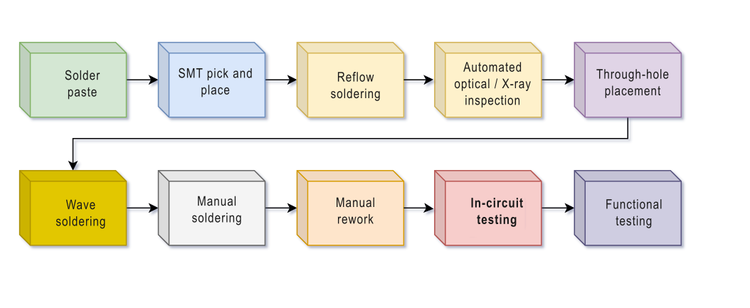
The process consists of the following main steps:
- Application of solder paste
- SMT placement by pick-and-place machines
- Reflow soldering
- Quality control using manual or automated optical inspection (AOI) as well as automated X-ray inspection (AXI)
- Through-hole component placement (if any)
- Wave soldering to solder through-hole component leads (if any)
- Manual soldering for delicate components and circuits
- Manual rework to fix any faults
- End-of-line quality control that includes in-circuit, boundary scan, and functional testing methods
Each of these steps can result in different types of defects as explained next.
What types of defects or issues can in-circuit testing identify?
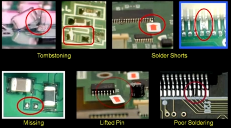
Some of the common PCBA defects include:
- Missing components: Due to an internal problem or drift in the pick-and-place machine, it may fail to place some components.
- Short circuits: Short circuits due to solder bridges between two closely spaced pins of an SMT IC can occur during reflow.
- Tombstoning: When one terminal of an SMT component is not soldered, it stands vertically like a tombstone.
- Lifted pins: Some IC pins can get bent and lose contact with the PCBA traces, resulting in unsoldered connections and open circuits.
- Poor soldering: The reflow and wave soldering processes are sensitive to temperatures, rate of change in temperatures, and motion. If these are not controlled correctly, there are chances of bad solder joints and unsoldered component leads.
- Wrong electrical properties: The capacitance, resistance, and inductance of some components may be out of specification due to a defective batch or a configuration mistake in the pick-and-place machine. In applications with high-frequency signals, even the lengths and spacing of traces, nodes, and vias can affect these properties.
What are the benefits of using in-circuit testing in quality control?
In-circuit testing boosts the overall production efficiency of PCBA manufacturing. Its benefits include:
- Higher productivity: Engineers can be sure that any functional problems are probably not due to fabrication defects and can focus on higher-level troubleshooting.
- High fault coverage: Its comprehensive electrical testing of the circuitry enables it to detect a wider range of potential design and manufacturing issues compared to visual checks.
- Component-level diagnosis: ICT checks individual components on the PCBA to identify the exact location and nature of a defect. This enables fast and accurate troubleshooting and repair.
- Support for complex PCBAs: ICT can be tailored to test complex assemblies accurately. Modern ICT systems can be adapted to conduct new tests and accommodate changes in PCBA design, offering flexibility to manufacturers as product designs evolve.
- Efficiency: ICT is a relatively fast and automated method that enables high-volume testing of PCBAs.
- Reduced rework costs: By catching defects early, ICT reduces the costs of reworking faulty PCBAs.
- Higher reliability: PCBAs that pass ICT are more likely to work reliably over their operational lifetimes, increasing the overall reliability of the final products and leading to higher customer satisfaction, better reputation, and reduced warranty claims.
- Cost-effectiveness: Although the initial setup cost for ICT can be high due to custom fixtures, its ability to identify a wide set of defects makes it a cost-effective quality control solution for the long term.
In-circuit test case studies
The following case studies demonstrate the above benefits for Keysight’s customers:
- Keysight in-circuit test systems reduced labor-intensive test tasks by 20% and increased throughput by 10% for testing printed circuit board assemblies of automotive advanced driver assistance systems.
- The PCBA test throughput of an auto parts maker went up by a factor of six.
- A global electronics manufacturer saw their test throughput boosted by a factor of four and saw significant cost savings.
How is in-circuit testing done on PCBAs?
Different test strategies and in-circuit testers are available. Let’s look at the different types of ICT and their test systems.
1. Bed-of-nails testing
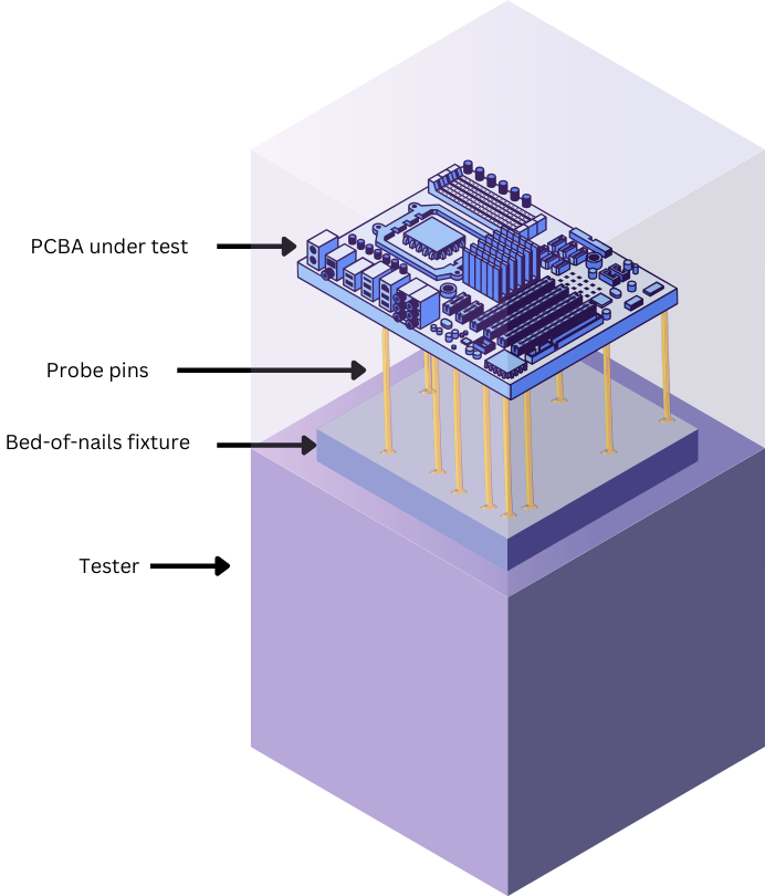
In this setup, a “bed of nails” test fixture, consisting of spring-loaded pins, is prepared such that the pin positions are aligned with the PCBA’s test points. When the PCBA under test is placed on the bed and pressed down, the pins make electrical contact with test points or component leads on the PCBA.
These contacts allow the tester to inject signals and power at specific points on the PCBA while measuring the electrical properties and responses, such as resistance, capacitance, and voltage levels. These readings are used to verify that components are correctly connected and to check for manufacturing defects like open circuits, short circuits, or incorrect component values.
The main drawback of this technique is that a fixture has to be custom-made for each PCBA layout under test and changed after each rework. Often, not just one but two fixtures are required for each layout — one for the top side of the PCBA and one for the bottom. However, good design for test (DFT) can ensure that all necessary test points are available on the same side and reduce fixture costs.
2. Flying probe testing
Flying probe testing is a far more versatile and dynamic technique. It consists of a set of movable probes that can be programmatically positioned at the test points for a particular electrical test. Test sequences are then programmed to move the probes, turn on power through some probes, and send electrical signals through other probes and the test points they are in contact with. Electrical properties are measured through the remaining probes too.
This programmable technique is more flexible, efficient, and productive than the static bed-of-nails approach.
3. Vectorless test extended performance (VTEP)
VTEP is not an alternative to the above two techniques but a complementary PCBA testing strategy to increase their test coverage. It’s particularly useful for detecting open circuit faults without requiring physical access or test points directly on the component leads.
VTEP uses special techniques to indirectly measure the capacitive signatures of components or solder joints and identifies potential defects through those measurements. This enables faster testing on dense PCBAs where probe-based or pin-based tests are challenging or impossible.
Using VTEP, manufacturers can improve their test strategies, achieving higher fault coverage and ensuring product quality without significant additional costs or complexities in the test process.
How is automated test equipment (ATE) used for in-circuit testing?
ATE systems are essential for high-volume in-circuit testing. They offer the following features and advantages:
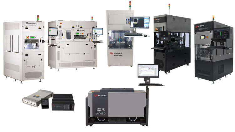
- Efficiency and productivity: ATE systems can have multiple ICT test cores to run multiple test sequences in parallel. For example, the Keysight i7090 massively parallel board test system has 20 ICT cores for parallel testing of multiple PCBAs.
- Complex testing capabilities: ATE systems are capable of testing modern complex PCBAs. For example, the Keysight i1000in-circuit test systems can test modern PCBA designs like high-speed digital interconnects and memory circuits and provide comprehensive coverage and diagnostics. The i1000 also allows the programming of protocols like the inter-integrated circuit (I2C) and serial programming interface (SPI), making it suitable for low-cost board testing with digital components.
- Flexibility: ATE models are available for both offline and inline configurations. For example, Keysight’s ATE solutions offer flexibility for PCBA manufacturers to integrate these systems into their production lines seamlessly.
- Industry 4.0 compatibility: Advanced ATE systems like the Keysight i3070in-circuit test systems support protocols like connected factory exchange, enabling integration into Industry 4.0 smart factories for improved machine-to-machine communication and data-driven decision-making.
- Graphical software configuration: ATE in-circuit systems offer powerful and user-friendly graphical software to configure the test sequences and automatically evaluate the test results.
What are some challenges and limitations of in-circuit tests?
Some of the challenges and limitations of in-circuit tests are outlined below:
- Limited access in complex PCBAs: High-speed and complex PCBAs often have limited test nodes to minimize unwanted signal interference, leading to low in-circuit test coverage. This requires additional testing methods, like boundary-scan testing, to ensure comprehensive test coverage without full access to the internal circuitry.
- High-frequency PCBA testing: High-frequency PCBA designs require careful consideration to preserve signal integrity, which may limit the effectiveness of ICT due to potential signal interference from test pads and close-running parallel traces.
- Production bottlenecks: The necessity for thorough test coverage and high accuracy can bottleneck the production line and affect the ability to efficiently meet demand.
- Measurement uncertainties: The pass or fail status of components during ICT depends on many factors like system residue, accuracy, resolution, noise ratio, compensation, fixture wiring, probe-to-board contact, and solderability. These factors introduce measurement uncertainties that can affect the accuracy and repeatability of ICT results.
- Variable component tolerances: Components like resistors, capacitors, and ICs may have varying tolerances due to differences in power rating, characteristics, and materials. These variances, along with other residual parameters like temperature, frequency, voltage, and circuit topology, can complicate the setting of appropriate test limits and the determination of criteria for pass and fail.
- Fixture and test probe challenges: The effectiveness of ICT is influenced by the design of the test fixture and the selection of the probe head styles.
- Programming challenges: In-circuit test programming requires consideration of tolerance multipliers, diode currents, fuse thresholds, fixture characteristics, and the precise setting of test limits. Adjusting the programming to achieve the desired accuracy and throughput while accommodating various test and system parameters can be challenging.
What advances and trends are emerging in the field of in-circuit testing?
Some of the advances and trends in ICT include:
- massively parallel testing
- advanced software tools like integrated program generators to increase test coverage, reduce debugging time, and improve test accuracy and repeatability
- use of boundary scan testing techniques for built-in self-test features within chips to increase coverage for devices that may be difficult to test using traditional ICT methods due to complex design or limited access
- advanced techniques like Monte Carlo methods for testing based on tolerance analysis
- enhancements in power supply performance for faster programming speeds
Can in-circuit testing be performed on complex multi-layer PCBAs?
For multi-layer PCBAs, test points of intermediate layers can be extended to the outermost layers to enable bed-of-nails or flying probe tests.
If the limited number of test points on high-density PCBAs cannot be easily reworked, cluster testing can be used instead. Cluster testing involves:
- automated cluster identification based on the bill of materials list and verification of cluster compatibility
- calculating acceptable impedance ranges for each cluster based on hardware requirements
- measuring the impedance of clusters to verify that they are within the acceptable ranges
In addition to ICT, other testing methods like X-ray inspection and automated optical inspection can be used to verify the correctness of the intermediate layers.
What are some common troubleshooting techniques used during in-circuit testing?
Common troubleshooting techniques include:
- Use of precision probes: They measure voltages, resistance, and signals at specific points to identify issues with power distribution, component values, and signal integrity.
- Isolating circuits: Temporarily isolating parts of the circuit can identify the location of a fault.
- Powering sections sequentially: Powering different sections of the PCBA sequentially can help to identify short circuits and excessive current draw.
- Signal tracing: Injecting known analog or digital signals into specific points and tracing how they propagate can reveal issues with signal paths.
- Boundary scan tests: For high-speed PCBAs with limited test nodes, boundary scan testing can check for defects without full access to internal circuitry, thus improving test coverage and minimizing the necessity for extensive functional tests.
- Tolerance analysis-based testing: Strategies that include tolerance multiplier adjustments, fixture characterization, and precise setup of global options per the specific requirements of the test can help in fine-tuning the test limits and minimize false test results.
Rely on Keysight in-circuit test systems for your PCBA quality control
In this blog, we dove into various facets of in-circuit testing during PCBA manufacturing. Keysight’s in-circuit test systems offer a range of capable and versatile testers for any use case and scale.