The field of electronic communications is rapidly expanding into every aspect of ordinary life. Detection, transmission, and reception of data require a wide array of devices such as optical sensors, RF MEMS, PIN diodes, APDs, laser diodes, and high voltage DACs, to name just a few. In many cases, these devices require several hundred volts to operate, calling for dc-to-dc converters that meet stringent efficiency, space, and cost requirements.
Analog Devices’ LT8365 is a versatile monolithic boost converter that integrates a 150 V, 1.5 A switch, making it ideal for high voltage applications found in the communications field, including portable devices. High voltage outputs are easily produced from inputs as low as 2.8 V and as high as 60 V. It features optional spread spectrum frequency modulation, which can help mitigate EMI, and many other popular features detailed in the data sheet.
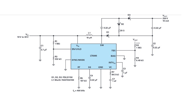
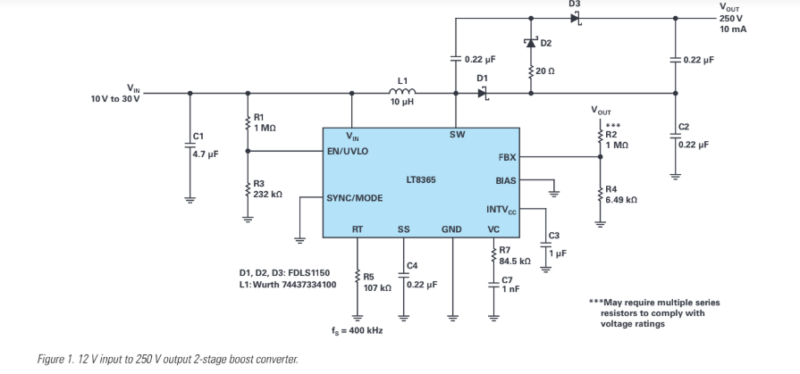
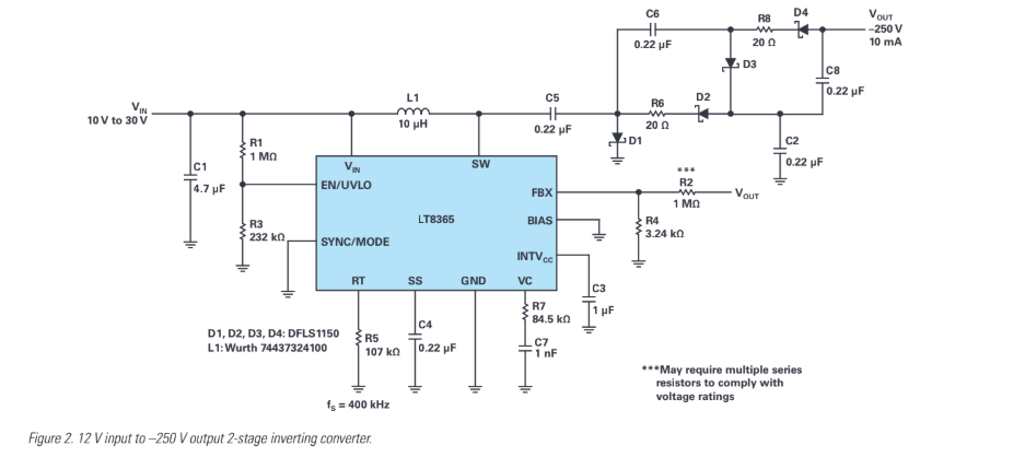
The converters shown in Figure 1 and Figure 2 have been used to provide the positive and negative voltage rails for high voltage DACs, MEMS, RF switches, and high voltage opamps, from a 12 V input source. These converters operate in discontinuous conduction mode (DCM) and deliver as much as 10 mA, with +250 V and –250 V output voltages with a conversion efficiency of about 80%.
Step-Up Ratios > 1:40
One benefit of DCM operation in a boost converter is the ability to achieve a high step-up ratio independent of duty cycle. Additionally, the values and physical sizes of the inductor and output capacitor can be reduced, which leads to a smaller overall footprint solution on the PCB. The circuit in Figure 3 can easily fit in an area less than 1 cm2.
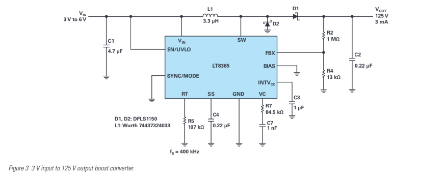 There are situations when only a very low input source is available and a high output voltage is needed. The converter shown in Figure 3 could be used to drive a variety of avalanche photodiodes, PIN diodes, and other devices requiring high bias voltages. This boost converter produces 125 V from a 3 V input source with up to 3 mA of load current.
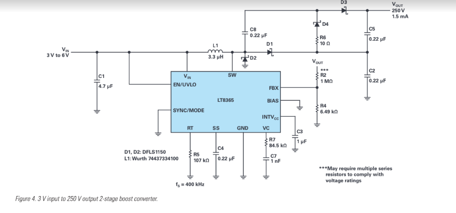
The converter shown in Figure 4 extends the 125 V output to 250 V from a 3 V input source and supports about 1.5 mA. There are many devices in the communications field requiring such high bias voltages from low input voltage sources.
How High or Low Can You Go?
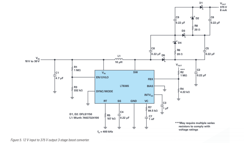
For situations where very high voltage is needed, whether positive or negative, a boost converter can use multiplier stages to boost the output 2×, 3×, or more. The converters in Figure 1 and Figure 2 show how to double the switch voltage in both directions, positive and negative. The 3-stage boost converter in Figure 5 delivers 375 V at 8 mA from a 12 V input source.
Note that the available output current must decrease as output voltage increases, since the switch capability does not change. As an example, a single-stage converter designed to deliver 20 mA will deliver about 10 mA when a second stage is added. As additional stages are added, always ensure the peak switch current stays within the guaranteed switch current limit.
Output Voltage Sensing Simplified
The LT8365 offers a single FBX pin to sense the output voltage. A simple resistor divider connected to the FBX pin senses the output voltage, independent of output polarity, as observed on all the schematics presented in this article.
Conclusion
The LT8365 enables applications that require compact, efficient, high output voltage boost conversion from input voltages as low as 2.8 V, which is common in the field of communications. It can also be used as an inverting converter and in popular topologies such as CUK and SEPIC converters. The LT8365 is available in a small, thermally enhanced, 16-lead MSOP package.
About the Author
Jesus Rosales is an applications engineer in Analog Devices’ Applications Group in Milpitas, CA. He joined Linear Technology (now a part of ADI) in 1995 as an associate engineer and was promoted to applications engineer in 2001. He has since supported the boost/inverting/SEPIC family of monolithic converters and some offline isolated application controllers. He received an associate degree in electronics from Bay Valley Technical Institute in 1982.

