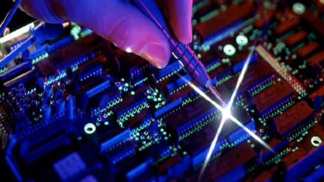
Printed circuit board (PCBs) have been an essential part of electronic gadgets for a long time. As we are stepping in the era of Smart industries the size of electronic devices is shrinking with unmatchable speed and performance. For maintaining the level of performance the components have to be placed with good isolation in PCB’s. As PCB is a first step towards starting any electronic circuit, knowledge of its do’s and don’ts are must be known. Let us find out how much you know about the world of PCB’s
- The tough work lasts only till an electrical schematic is complete
A blueprint is drawn first before starting the real circuitry. In electronics, this blueprint is coined as electrical schematic which looks like simple but its hardware implementation is challenging. Generally placing the required components with appropriate connections seems easy but the physical design constraints (size and placement of the parts, orientation of parts on opposite side of PCB), the electrical interaction between signals, heat dissipation, and signal loss through the wires/traces are the main factors to be considered.

- How mounting technology changes from prototyping to production
Depending on the intent of your design, you may make vastly different choices in the types of components to be used and how they are placed. One can select through-hole technology that is easy to solder in PCB and relatively inexpensive but once the design goes for production line the choice changes to Surface-mount parts as it does not require as many as drilled holes which restore the compactness factor. SMT resolves the space problem as it does not have leads they are directly mounted to PCB’s.
- Take care of Physical size and distance of components
In order to get a functional circuit from the prescribed design layout, it is necessary to place the components in close proximity in the layout as designed in the schematic. Designed schematics is different from the real components designing in the PCB, so in order to avoid functionality hack the Physical dimension of the components and their locations from neighboring boards.
- Proper management for Distributing Power
Proper distribution of power from power supply component or from the board has to be taken in account in order to check the performance of the circuit. Power can be supplied in different ways but regardless of methods, its interconnections have to be sketched out in order to supply proper current to each component avoiding chopped-up power plane.
 PCB manufacturer not necessary can build it as perfect as you can design it
While starting designing one must also take care of the manufacturer from whom PCB is purchased. A perfectly manufactured PCB increase the success ratio of PCB design. In order to buy reliable and cheaper PCB board, its genuine players must be known. DFM (Design-for-manufacturability is another analysis done by manufacturers on completed design as early as possible. In this case if manufacturer calls for the improvement it is going to be worth effort to make changes in design slightly in order to produce required product.
- Little efforts can make a huge difference in the design
Even a smaller mistake can turn your complete design a disastrous. There is always a difference between analyses of components physically when compared to their technical respective datasheet. All the parts libraries do not necessary matches. Many a time the size of a component, the proper assignment of pin and spin orientation also matters. Always take care of the components matches to the datasheet.
- Logical placement of components is essential.
As discussed earlier the distance and proper placement of components is very important for a design to work properly. It does not mean that assembling similar components into a common area is the best way to reduce space constraints in the PCB. The components have to be placed in relative proximity in order to maintain the losses due to different reasons. It is really necessary to place the component logically.
- Routing should be measured under all aspects.
One cannot rely completely on the auto-router for the placement of components. It is not always necessary. Many a times when auto routed board is used it may connect all the required points but it is not necessary it will electrically perform well as assumed. Make a proper routing of power, ground and the difficult nets and then run the auto-router software in order to avoid any discrepancy.

- Usage of trace width calculator to simplify design
Trace width is also the important factor and should be taken care of while routing. Trace width is governed by impedance requirements offered by high-speed lines. A load with high current have to be sized large in order to avoid the issue of overheating which often damages the components. In order to avoid the damage, the current load of power net must be taken into consideration. In order to make calculation easier usage of trace width calculator can be implemented.
- Every tool has some limitations
Good engineering practices can not be compromises in the shades of tools. The Design Rule Check can only provide validation of certain points but they do not always ready to determine dimensions, path length and trace geometry in order to get required electrical specifications.


