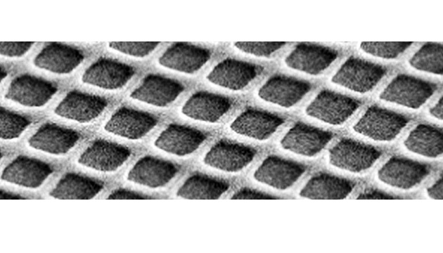
A new technique named laser shock imprinting has been used by researchers from Purdue University, the University of Michigan and the Huazhong University of Science and Technology. This technique will permanently stress grapheme into having a bandgap, which makes graphene useful for various electronic components.
A laser was used to create shock wave impulses by the researchers, which penetrated an underlying sheet of graphene. The graphene was stretched onto a permanent, trench-like mold, by the laser shock.
This caused the widening of band gap in graphene to a record 2.1 electronvolts. Previously, scientists achieved 0.5 electronvolts, barely reaching the benchmark to make graphene a semiconductor like silicon.
“This is the first time that an effort has achieved such high band gaps without affecting graphene itself, such as through chemical doping,” said the paper’s corresponding author Gary Cheng, professor of industrial engineering at Purdue University.
There is still a way to go before turning graphene into a semiconducting device, but the technique provided more possibilities in taking advantage of the material’s optical, magnetic and thermal properties, according to the team.


