Pulsonix, the Electronic Design Automation (EDA) company delivering technology-leading PCB design solutions, announced the release of Pulsonix version 10.5, with over 30 new enhancements based on user requests from professional PCB designers. “We are very connected with our customer base, giving us lots of input on how to help them achieve their design goals more quickly and efficiently,” said Bob Williams, marketing director for Pulsonix.
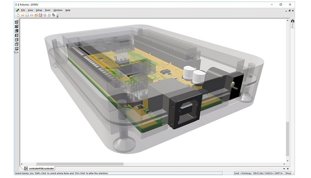
“One common theme led us to implement an intuitive 3D collision detection, measurement, and editing system that makes it easy to find and visualize 3D spacing problems and then fix them in the same 3D environment,” he added.
PCB design created strictly in a 2D environment makes it very difficult to avoid physical spacing problems caused by part packages, board enclosures, or other non-electrical components, which is inherently a 3D problem. The Pulsonix 10.5 release includes new 3D viewing options for component and enclosure transparency, lighting, and clash markers, and component-to-component distance measurements. Users fix problems in the 3D environment by repositioning objects in single-axis movements, making it very easy to move components while also maintaining proper alignment with the board and other components.
Beyond fixing problems, the new 3D exploded view enables users to visually inspect the via structures and copper of internal layers of multi-layer PCBs. Finally, for precise and intuitive view positioning, Pulsonix now supports a 3D SpaceMouse, allowing users to rotate and zoom the view simultaneously with one hand, while the other uses the mouse to make component positional changes.
Another area of commonly requested improvements involved design rules and constraints. New for the 10.5 release is the ability to define constraint rules by area in the schematic around components and nets, and then propagate those rules to the PCB environment. Users can also gain improved control with the ability to turn on or off individual rules, seeing which rules are being violated in a single table view, spreadsheet style filtering of rules, and other convenience features.
User requests led to improvements in many other areas of the Pulsonix toolset. For example, track impedance tooltips now make it fast and easy to see the impedance, capacitance, inductance, and propagation delay for any track on the PCB. Another example is the new bus connection and multi-net routing capability in the schematic editor.
“The Pulsonix 10.5 release adds convenience and improves design time in so many areas,” said Olaf Hollinger at Carl Zeiss AG. “I especially appreciate the new schematic area definitions. With this, we can now easily define the constraint rules earlier in the design process and utilize them in the PCB design. This will be a great asset to our designs.”
To see a complete list of all the enhancements to the Pulsonix 10.5 release, visit www.pulsonix.com/latestversion
For more information, visit: www.pulsonix.com


