New Concept Creates All-in-One RGB MicroLEDs, Eliminates Several Transfer Steps to Receiving Substrate & Boosts Performance
Leti, a research institute of CEA Tech, announced a new technology for fabricating GaN microLED displays for applications ranging from smart watches to TVs with no size limit.
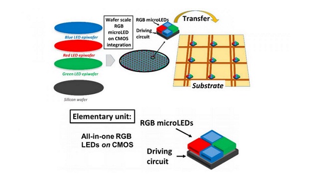
The approach fabricates elementary units of all-in-one red, green, blue (RGB) microLEDs on a CMOS driving circuit, and transfers the devices to a simple receiving substrate. The units are fabricated with a full semiconductor, wafer-scale approach.
“This new process, in the proof-of-concept stage, paves the way to commercial, high-performance microLED displays,” said François Templier, CEA-Leti’s strategic marketing manager for photonic devices. “The CMOS-based approach provides higher brightness and higher resolution microLEDs and is a game changer for very large TVs.”
While they promise exceptional image quality and better energy efficiency than existing liquid crystal display (LCD) and organic light-emitting diode (OLED) technologies, microLED displays currently face significant barriers on the road to commercialization.
One of the biggest challenges is improving the performance of the driving electronics, which require more power to deliver brighter images and more speed to support continuously increasing demands for high display resolution. Faster electronics are required to power millions of pixels in a fixed-frame time in microLED displays, but existing driving display technology, known as a thin-film transistor (TFT) active matrix, cannot provide the necessary current and speed.
CEA-Leti’s new approach fabricates CMOS-driven, high-performance GaN microLED displays with a simplified transfer process that eliminates the use of the TFT backplane. RGB microLEDs are stacked directly onto a micro-CMOS circuit, and each unit is transferred onto a simple receiving substrate. Then, the RGB microLEDs and the backplane are fabricated on a single semiconductor line.
In addition to increasing power and driving speed – and improving display performance – this process avoids several costly steps needed with current technology to make electrical and mechanical contacts between micro-LEDs and the receiving substrates.
CEA-Leti presented a paper on the breakthrough titled “A New Approach for Fabricating High-Performance MicroLED Displays” on May 14, during Display Week 2019 in San Jose, Calif.
For more information, visit: www.leti-cea.com


