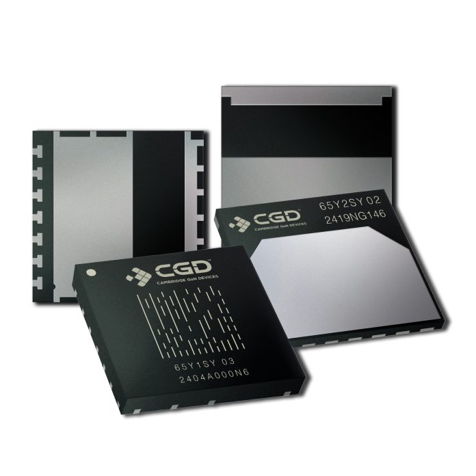
Cambridge GaN Devices (CGD) has launched two new packages for their ICeGaN family of GaN power ICs. These new packages are designed to enhance thermal performance and simplify inspection, targeting applications in data centres, inverters, and more. Variants of the well-proven DFN style, both packages are noted for their extreme ruggedness and reliability. This development supports CGD’s mission to make greener electronics possible through innovative semiconductor technology.
- DHDFN-9-1 (Dual Heat-spreader DFN)
Design: Thin, dual-side cooled package with a 10×10 mm footprint.
Features:
- Wettable flanks for simplified optical inspection.
- Low thermal resistance (Rth(JC).
- Flexible cooling options: bottom-side, top-side, and dual-side.
- Dual-gate pinout for optimal PCB layout and easy paralleling.
Advantages: Outperforms the TOLT package in top-side and dual-side cooling configurations, supporting applications up to 6 kW.
- BHDFN-9-1 (Bottom Heat-spreader DFN)
Design: Bottom-side cooled package with a 10×10 mm footprint.
Features:
- Wettable flanks for easy inspection.
- Thermal resistance of 0.28 K/W, matching or exceeding other leading devices.
- Similar footprint to the TOLL package, allowing for a common layout and ease of evaluation.
Benefits of Improved Thermal Resistance
- Increased Power Output: More power at the same RDS(on).
- Lower Operating Temperatures: Devices run cooler for the same power, reducing heatsinking needs and system costs.
- Enhanced Reliability: Lower temperatures lead to higher reliability and longer lifetimes.
- Cost Efficiency: Designers can use lower-cost parts with higher RDS(on) while achieving the required power output.
These advancements in packaging technology enable the GaN power ICs to offer superior performance, reliability, and cost-effectiveness, contributing to greener and more efficient electronic solutions.

