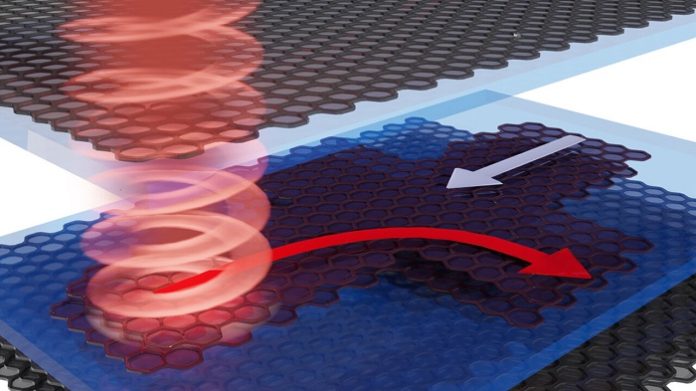
The way electrons flow in a material determines its electronic properties. For example, when a voltage is sustained across a conducting material, electrons start flowing, generating an electrical current. These electrons are often thought to flow in straight paths, moving along the electric field, much like a ball rolling down a hill. Yet these are not the only trajectories electrons can take: when a magnetic field is applied, the electrons no longer travel in straight paths along the electric field, but in fact, they bend. The bent electronic flows lead to transverse signals called “Hall” responses.
Now, is it possible to bend electrons without applying a magnetic field? An international team of researchers reports that circularly polarized light can induce bent electronic flows in bilayer graphene. The study has been carried out by a team including ICFO scientists Jianbo Yin (currently, a researcher from the Beijing Graphene Institute, China), David Barcons, Iacopo Torre, led by ICREA Prof. at ICFO Frank Koppens, in collaboration with Cheng Tan and James Hone from Columbia University, Kenji Watanabe and Takashi Taniguchi from NIMS Japan and Prof. Justin Song from Nanyang Technological University (NTU) in Singapore.
Jianbo Yin, the first author of the study, remembers how it all started. “This collaborative study began in 2016 with a conversation between Justin Song and Frank Koppens at a scientific conference.” As Justin Song explains, “Electrons are not just particles, but can have a quantum wave-like nature.” In quantum materials, such as bilayer graphene, the wave pattern of electrons can exhibit a complex winding often referred to as quantum geometry. “Frank and I talked about the possibility of harnessing quantum geometry in bilayer graphene to bend the flow of electrons with light instead of using magnetic fields.”
With this in mind, Jianbo Yin, a researcher in Frank Koppens’ team, decided to take on the challenge of experimentally realizing this unusual phenomenon. “Our device was very complicated to build. It took building many devices and flying to Columbia University to work with Cheng Tan and James Hone to improve the device quality.”
Quantum geometry and valley selectivity
In bilayer graphene, there are two pockets of electron valleys (K and K’): when a perpendicular electric field is applied, the quantum geometrical properties of electrons in these two valleys can cause them to bend in opposite directions. As a result, their Hall effects are canceled out.
In their study, the team of scientists found that by applying circular polarized infrared light onto the bilayer graphene device, they were able to selectively excite one specific valley population of electrons in the material, which generated a photovoltage perpendicular to the usual electron flow. As Koppens highlights, “We now engineered the device and setup in such a way that current only flows with light illumination. With this, we were able to avoid the background noise that hampers measurements and achieve sensitivity in the detection several orders of magnitude better than any other 2D material.” This development is significant because conventional photodetectors often require large voltage biases that can lead to “dark currents” that flow even when there is no light.
Yin remarks that “we can control the bending of the electrons with the out-of-plane electric field we apply. We can change the bending angle of these electrons, which can be quantified by the Hall conductivity. By controlling the voltage ‘knob,’ the Berry curvature [one characteristic of quantum geometry], can be tuned, which can lead to a giant Hall conductivity.”
The results of the study open a new realm of many detection and imaging applications, as Koppens finally concludes. “Such discovery could have major implications in applications for infrared and terahertz sensing since bilayer graphene can be transformed from semimetal to semiconductor with a very small bandgap, so it can detect photons of very small energies. It may be also useful, for example, for imaging in space, medical imaging, e.g. for tissue skin cancer, or even for security applications such as the quality inspection of materials.”
The possibilities are manifold and the next steps of research focused on new 2D materials, such as the moiré material twisted bilayer graphene, may find new ways of controlling electron flows and unconventional optoelectronic properties.

