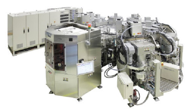
ULVAC, Inc. announced the successful launch of PZT piezoelectric thin-film sputtering technology and a high volume manufacturing (HVM) solution to solve technical issues that have hindered the development of MEMS devices, which are crucial in applications from autonomous driving to next-generation wearable terminals (such as smart glasses). The company has begun selling production systems incorporating the new technology.
Evolutions in technologies such as 5G and AI are expected to accelerate the journey towards smart societies, in which the digitization of all types of industries will improve industrial performance and enhance convenience for people. With increasing levels of multi-functionality found in autonomous driving, AR/VR, security, and smartphone applications, actuators are needed in order to activate devices based on signals received from various types of sensors. Demand for actuators is projected to explode and key issues in their development have come to the fore, including the need for miniaturization, reduced production costs, lower power consumption, and higher performance.
It used to be impossible to fabricate PZT piezoelectric thin films, which constitute the key technology in sensors and actuators, using a low-temperature process with the conventional coating method (Sol-Gel). However, in 2015, ULVAC successfully developed the world’s most advanced technology for forming PZT piezoelectric thin films using a low-temperature sputtering process. ULVAC has continued developing this as next-generation MEMS technology.
By further advancing this proprietary technology, ULVAC has reduced running costs by optimizing system operation and has greatly improved the technology’s reliability, which is critical for device commercialization. The result is a groundbreaking mass-production technology that is now incorporated into systems ULVAC has begun to sell.
This technology allows MEMS devices to be integrated with semiconductors (CMOS), and enables other positive outcomes such as miniaturization, reduced production costs, lower power consumption, and higher performance. It is expected to pave the way for increased use of MEMS devices in sensors and actuators in spatial information sensing and 3D image displays, including smart glasses. The technology will also facilitate MEMS device use in applications such as 3D fingerprint authentication.
ULVAC will continue to spearhead innovations in MEMS device technologies that can be used in a wide range of applications, including etching, sputtering, ashing, and sputtering targets. With all of these contributions, ULVAC plans to remain a driving force in the creation of smart societies.
For more information, visit: www.ulvac.co.jp/en/


