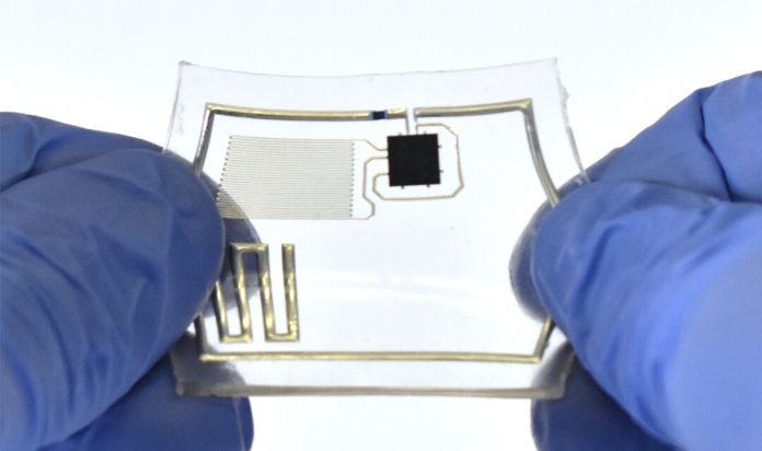
Carnegie Mellon mechanical engineering researchers have developed a new scalable and reproducible manufacturing technique that could accelerate the mainstream adoption and commercialization of soft and stretchable electronics.
The next generation of robotic technology will produce soft machines and robots that are safe and comfortable for direct physical interaction with humans and for use in fragile environments. Unlike rigid electronics, soft and stretchable electronics can be used to create wearable technologies and implantable electronics where safe physical contact with biological tissue and other delicate materials is essential.
Soft robots that safely handle delicate fruits and vegetables can improve food safety by preventing cross-contamination. Robots made from soft materials can brave the unexplored depths of the sea to collect delicate marine specimens. And the many biomedical applications for soft robots include wearable and assistive devices, prostheses, soft tools for surgery, drug delivery devices, and artificial organ function.
But creating these nearly imperceptible components that can seamlessly integrate with human life is only the first step. Mainstream adoption and commercialization of soft and stretchable electronics will require the development of new manufacturing techniques that are scalable and reproducible.
Although a variety of methods have already demonstrated the ability to fabricate liquid-metal-based devices on a smaller scale in labs, these methods have not yet resulted in the critical combination of desired features required to produce liquid-metal-based soft and stretchable electronics at a commercially viable scale.
A team of researchers from Carnegie Mellon University’s College of Engineering seeks to change this with a novel method they have developed for mass manufacturing of liquid-metal-based soft and stretchable electronic devices.
Kadri Bugra Ozutemiz, who recently earned his Ph.D. in mechanical engineering, has developed a new approach that achieves scalability, precision, and microelectronic compatibility by combining the use of liquid metal with photolithography and wafer-based dip coating.
Ozutemiz, who worked with Carmel Majidi and Burak Ozdoganlar, both professors of mechanical engineering, explains that liquid metals have become popular in recent years as a conductor for stretchable circuits to create sensors and antennas as well as soft and stretchable wiring for various electronics and robotics applications.
The gallium-based alloy, eutectic gallium–indium (EGaIn), is liquid at room temperature, can freely flow inside channels, has high electrical conductivity, and can be deformed as long as it is encapsulated in another medium.
“We had to better understand the inherent properties of gallium-based liquid alloys to overcome challenges that make them unsuitable for mass manufacturing,” said Ozutemiz.
The most significant challenge was that a thin gallium-oxide “skin” rapidly forms when the liquid metal is exposed to air, which makes it difficult to achieve a uniform and continuous shape or geometry. The liquid metal sticks everywhere, flowing into a wide variety of changeable shapes.
“Our team devised a novel approach that combines selective metal-alloy wetting that deposits the liquid metal into the desired circuit layout with a dip coating process that dissolves the oxide skin that results when EGaln is exposed to the air,” explained Ozutemiz.
Thin metal traces, made of affordable and readily available copper, are first lithographically patterned onto an elastomer surface as a wetting layer. The traces serve as templates for selectively depositing the EGaln onto the silicone rubber surface.
In order to dissolve the oxide skin while maintaining the selective deposition of the liquid metal, the researchers devised a novel approach that combined the selective metal-alloy wetting with a dip coating process.
Dip-coating, which has been used in the microelectronics industry, but not with liquid metals, facilitates the deposition of EGaIn selectively onto the circuit layout defined by lithographically patterned copper traces on elastomer-coated wafers in a scalable manner.
An automated, high-precision motion system and a two-layer dipping bath are used to deposit the EGaIn onto the patterned copper wetting layer. The bath includes a thin layer of aqueous sodium hydroxide (NaOH) solution at the top surface, followed by the EGaIn. The NaOH solution facilitates the removal of oxide skin and of any oxidation on the surface of the copper traces when the patterned wafer is dipped into the bath. The wafer is then immersed into the bath, and after a short dwell time, is withdrawn at a prescribed speed that controls the amount of liquid deposited on the substrate.
The researchers used a custom-built simple machine to dip the wafers into the bath. By controlling the withdrawal speed, they successfully produced repeatable liquid metal geometries.
In future testing, they will work to control parameters such as withdrawal speed and the amount of time the wafer remains in the bath in order to better understand what affect each variable has on the resulting geometry. But for now, they have established a viable process for the mass production of liquid metal circuits that can be used in a wide variety of soft robotic and electronics applications.
“For us, what was most important was that we achieve repeatable results with a standard process that is already used by chip manufacturers,” said Ozutemiz, who explained that by introducing a new material into a well-established process, manufacturers will be able to scale production that will allow for more widespread adoption of these innovative soft robots and electronic devices.


