Introduction
Companies are always working on the next big technology that will propel the world forward. Without a doubt, the biggest breakthroughs have occurred in the information age with advances in telecommuni- cations and data transfer. Buzzwords like 5G, 6G, IoT, machine-to-machine (M2M) communication, and machine learning are used every day to describe where the world is heading. The world has become smaller as everyone and, in some respects, everything is being connected.
To accomplish such a monumental goal, research and development (R&D) teams around the world are tasked with finding more efficient ways to move data. One of the challenges engineers face is the volume of data and the channel bandwidth that is needed to move such large amounts of data. It is no secret and trends are showing the only real way to proceed, is to move the frequency of operation higher into the millimeter-wave (mmWave) bands.
The concept for higher frequency moving more data can be complicated. Consider bandwidth (maximum amount of data transferred over a given path) as a percentage of the carrier frequency. This would imply that the higher a carrier frequency is, the larger the bandwidth. Data rate (data transmitted per unit time) is a function of bandwidth. In simplest terms, higher frequency leads to higher bandwidth and that leads to larger data rates.
Another reason a move into the mmWave bands is important is because there is more swaths of contiguous BW available in the mmWave bands, thus you can support wider BW modulation in a single carrier, whereas the lower frequency bands are over-crowded and can’t support the wider single carrier bandwidths required for massive data thruput. That is not to say interference cannot happen, it is just fortunately there are a fewer reasons that help to keep interference to a minimum. For example, the signals in the mmWave bands do not propagate as far due to much higher path losses and the likelihood of PIM affecting receive bands is lower due to both the higher propagation losses and the fact that the 3rd, 5th, and 7th order PIM signals will, in general, be very far from defined receive bands.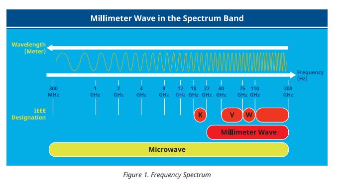
What does mmWave development mean? Well, mmWave is defined as the frequencies between 30 GHz to 300 GHz (figure 1). In practical applications, many engineers will sometimes refer to mmWave as operation in frequencies higher than 70 GHz. It is obvious why mmWave frequencies will support future data transfer needs, but not without novel equipment, engineered to be at the forefront of this technological leap.
As these device developments are engineered and begin to mature in the +100 GHz application space, they are not without challenges. Challenges not only in the hardware that supports these applications but also in the measurement setups and measurements themselves. One such challenge for measurements over 100 GHz exists in the calibration of Vector Network Analyzers.
This application note will explore the need for broadband amplitude calibrations from low frequency to 110 GHz as well as challenges for making such broadband measurements in both frequency and amplitude. It will also cover how to overcome these challenges. The final portion of this application note will provide a procedure for conducting a broadband calibration using the Power Master MA24510A and VectorStar Vector Network Analyzer ME7838A.
Why are Power Measurements for a Device Characterization Important?
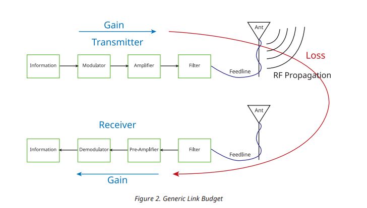
Power is a fundamental property of a device, especially amplifiers and active devices, which provide gain to signals that need more power. Precise knowledge of power performance of the various amplifying devices is necessary to prevent damage to devices that are receiving the amplifier output as well as to ensure proper input power to the amplifier, reliability, and signal fidelity. Many RF devices are usually part of a larger system and that system generally has some type of accounting of power moving from one section to another. For many telecommunication systems, this is referred to as a link budget and is a tool for measuring signal quality as it relates to the signal-to-noise ratio (SNR).
 As mentioned earlier, device damage is a real concern for designers, so power levels must be known for all active devices. While this may seem trivial, measurement products that are broadband can be quite sophisticated in the hardware architecture. If not properly calibrated, the measurement product can introduce various power levels from low to high frequencies due to band switch points and other hardware. This can cause damage to the devices. Aside from device damage, there are a lot of parameters that require power measurements to be accurate. Not only does telecommunications applications use mmWave transceivers, automotive radar applications also use mmWave transceivers and rely on associated power measurements.
When a designer needs to add an amplifier to a product, the limitations of the amplifier will be sought. Before limitations can be determined, there should first be an emphasis of keeping an amplifier in the linear region for operation. The amplified needs to be in the linear region to avoid compression as well as frequency harmonic generated signals that can interfere with the intended signal.
Next we want to focus on characterization of the amplifier to identify limitations. Limitations like the 1 dB compression point (P1dB) can provide information about what power level an amplifier is no longer amplifying a signal due to compression. Another common test for the amplifier is intermodulation distortion (IMD) which tests the harmonic output based on a two-tone input. This test is used to make sure the amplifier does not introduce signals and amplifies signal harmonics in an application. In order to get the most accurate IMD measurement, the input power must be known as this information is used to the third-order intercept (TOI). Again, these parameters are important and require accurate power measurements.
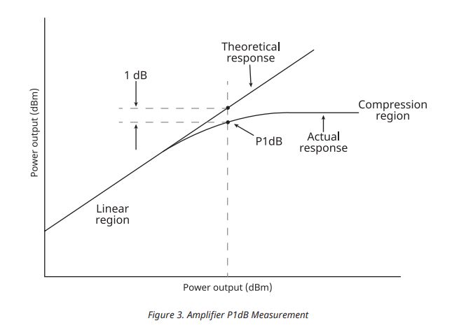 While this discussion has focused on parameters based on the maximum output of the amplifier, many applications also require very low signals and the swing of levels in between both extremes. The telecommunication market and lots of those applications use very low signals, many lower than -30 dBm and some as low as -90 dBm. Technology has made signals this low easy to create, but there are some challenges around calibrating a test system that can produce and receive these low signals accurately.
What Should the User Know About the Calibration?
Vector network analyzers (VNAs) are the default test equipment used for active device testing. Manufacturers of these instruments offer the ability to test power parameters through a source and receiver architecture along with many other useful measurements. These systems generally have generic accuracy for various S-parameter and power measurements, but also have the ability to calibrate the source and receiver based on the test requirements. One such question that comes up is, “why does anyone need to do a calibration before testing a device if the test equipment is new and just came from the factory?” or “isn’t the factory calibration good enough?”.
This is a fair question and in many cases, the instrument may provide accurate results for a majority of measurements. There are many setups, however, they require higher accuracy of interpolation in both frequency and power axes. The other major reason for a user calibration is to move the power measurement away from the test port and establish a power reference plane in a desired location.
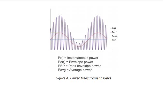
There are many types of power sensors on the market that are differentiated by internal architectures as well as measurement capabilities. While there are many types of measurement capabilities, a simple average power calibration will suffice (figure 4).
With so many types of power measurements available, an average calibration is enough to give the right accuracy for the various measurements across a large frequency range. The simple answer is yes.
Challenges with Broadband Power Calibrations
Many users of VNAs that measure active devices are most likely familiar with common practices of doing power calibrations via a power sensor. While this is very common and users may not experience any challenges for low frequency calibrations, challenges can present themselves when doing the same operations in the mmWave frequencies. Challenges like complete frequency coverage of the instrument, automatic level control trade-offs, calibration time, and voltage standing wave ratio (VSWR)/ accuracy across frequency can all be present when performing a broadband calibration up to 110 GHz.
Frequency Coverage
For many users, there is nothing more frustrating than having test equipment that can cover the frequency range of interest, only to be limited by components and/or equipment necessary for calibrations and operation. Many times, users must resort to using a low frequency power senor and a high frequency power sensor to accomplish a broadband calibration. Obviously this is not an ideal solution because of the cost of two sensors and it can be a time consuming effort.
Level Control Coverage
Another challenge for test engineers, R&D engineers, and manufactures is the lack of available calibrated automatic level control (ALC) to address power requirements. Unlike the previous example where there exists a lack of broadband frequency coverage, there is also the issue of power level coverage. Many applications can have a low power requirement, high power requirement, or both. While an instrument may be able to address the power requirement range, customers may become confused and annoyed that the power sensor reliable for calibration can become non-responsive during the calibration. This is generally due to the sensor’s inability to resolve power levels for extremely low signals or for signal bandwidth that may be too large to cover all the desired power levels.
Voltage VSWR and Accuracy
VSWR should always be a concern for any measurement. This measurement is an indicator of how efficiently power is being delivered to a system. A well- known challenge for many RF systems and components is keeping a good VSWR specification over a very broadband frequency set, especially up to 110 GHz. The main issue is that VSWR deteriorates as the frequency climbs higher than 90 GHz in most well-designed RF systems.
Poor VSWR can have a direct impact on measurement accuracy, which is a key merit for any test system and can be the deciding concern for a purchase of one piece of equipment over another. For power measurements, accuracy is crucial and cannot be ignored. Fortunately, there are ways to improve accuracy for test systems including power sensors that are available for users.
Calibration Time
Time to market is a real concern for any manufacturer and as 5G and 6G progress, this idea will only become more important. Because power measurements are a requirement for amplifiers, especially for the receiving and transmitting sides of a transceiver system, measurements should be as fast and accurate as possible. Assuming a user can get the full frequency and ALC levels corrected, the issue of time for a calibration can come into play. While the time may seem trivial for a calibration, the amount of time over the course of year can become considerable, especially for custom calibrations that require lots of points across a broadband frequency set.
Cost
There is no way to avoid the conversation of cost because it is a well-known fact that cost can increase steeply as one moves up in frequency for R&D and/ or testing. Customers are continuously challenged with having to find a product that fits in their budget but also has decent performance. Many times, cost of a product can become the sole contributor for a customer considering a product.
Technologies for Calibrations
When conducting calibrations with power sensors, there are some options with differing technologies. thermal sensors and receiver-based Non-Linear Transmission Line (NLTL) sensors are both available up to 110 GHz but there are some stark differences and trade-offs between both technologies.
For thermal sensors, there are a couple of approaches for thermal sensing. A Wheatstone bridge with a thermistor can be used to sense RF power. The RF energy is applied to the thermistor, a change in temperature is detected, and a change in resistance can quantify the power level. Another approach for sensing power is by utilizing the Seebeck effect in which dissimilar materials are joined together at one end and a potential difference is produced when the junction changes temperature. Like the former example, changes in the temperature can allow the characterization of power through the device. Figure 5 shows a couple of diagrams of thermal sensing technologies.
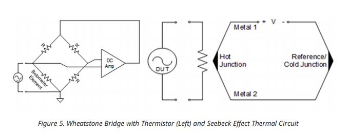 This technology is widely used and features the best accuracy for power sensors. There are some trade-offs to this technology like slow settling times which translates to an overall increase in calibration time. This may not be an issue for small frequency coverage but over large frequency bandwidths, 9 kHz to 110 GHz, time consideration can be important. A long calibration time can also affect overall thruput in manufacturing because calibrations time can add up over the course of a year or longer.
Another limiting feature of this technology is level control coverage. As mentioned earlier, a user may want to conduct thorough testing of a device under test (DUT) and the power level range may warrant -50 dBm to +10 dB for example. Thermal sensors are limited to approximately -30 dBm. This technology may not adequately address manufacturing or design concerns.
One important distinction that should be made is that thermal sensors look at integrated power. This means that a thermal sensor will see all signals like source harmonics for instance. Depending on the application, this may be useful but will fall short on applications that require an emphasis on fundamental power.
Advantages of Using Power Master MA24510A
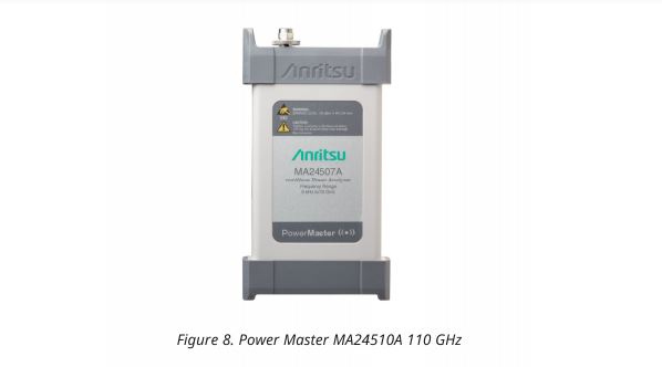
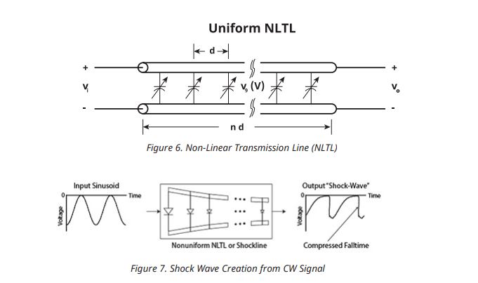
The Power Master MA24510A has many advantages that addresses customer challenges. In many parts, this is due to the design of the Power Master. Unlike other power sensors, the Power Master MA24510A has an architecture similar to a spectrum analyzer. The Power Master has a receiver-based design that can accurately evaluate power through an RF sampler. This architecture also allows the MA24510A to use NLTL to scale high to low frequency.
NLTL is a pseudo-transmission line where voltage-dependent varactor diodes are in place where a shunt capacitor would exist on a standard transmission line (figure 6). When voltage (CW signal) is applied across the NLTL, a shock-wave is produced and based on the applied voltage, the incident wave compresses the fall time on the shock wave creating a train of very narrow gating pulses that feeds into a sampler and can be used to characterize power (figure 7). These pulses contain harmonics with nearly the same power as the fundamental frequency and can be multiplied to provide input power levels across a broad frequency range of 9 kHz to 110 GHz.
 There are many challenges that customers face that highlight advantages to using the Power Master MA24510A.
- Frequency and Level Control Coverage
- VSWR and Accuracy
- Calibration Time
- Cost
NLTL implementation also allows for level control coverage down to -90 dBm and up to +23 dBm, the largest level control coverage on the market. This is where thermal sensors are limited to around -30 dBm to +10 dBm. To be completely fair, the VectorStar can utilize level control from -40 dBm up to +23 dBm, much better than that of a thermal sensor.
Calibration time is also another customer challenge that can be alleviated through NLTL because NLTL technology does not rely on physical changes. Physical changes can take several seconds per minute to settle and report in the sensor to create a good power characterization. Calibration time can also be reduced because the broadband nature of the Power Master does not require the user to switch between power sensors and corresponding power meters to access frequency coverage from 9 kHz to 110 GHz.
Cost may be the biggest advantage for the Power Master MA24510A because NLTL is implemented as a System on Chip (SoC) and that greatly reduces cost to the customer while simultaneously reducing temperature variation across reflectometer constituents. This translates into greater stability over time and longer intervals between calibrations, increased accuracy, and repeatability.
Accuracy for fundamental power is another advantage of the Power Master. Thermal sensors measure integrated power which will see harmonics as well as the fundamental. The Power Master focuses on fundamental power and will provide more accuracy for users that require a controlled measurement of fundamental power during calibrations.
The Power Master MA24510A can address many of the challenges described earlier because it uses NLTL.
Trade-Offs
For any product that is new and novel in the market and operates to 110 GHz, users can expect a certain performance level with key specifications. To get to electrical specifications, either VSWR or frequency scalability, trade-offs are always a part of the design process. Keep in mind that designing any one specification for the best performance is difficult and instruments are generally designed as the best performance as the sum of the parts. It is true that some specifications may not be easily improved, but with some insight, users do not always have to accept specifications and can improve them as needed.
It may seems like magic that a power sensor can accomplish the outer boundaries of frequency and power coverage and still maintain good performance. While no such magic exists, internal components all contribute to performance, especially VSWR. With such a mess of networks all striving to reach the absolute best VSWR, sometimes the reality is that feat may not be easily had.
Not all specifications are equally created and Anritsu has been known to be on the conservative side of specifications. This means that VSWR, which directly affects accuracy, can seem good for some applications and not so good for other applications. Fortunately, there are ways to externally improve the VSWR and accuracy of the Power Master MA245110A, if such performance is warranted.
One such way is to add a fixed attenuator to the input of the Power Master. The fixed attenuator would need to be broadband, ideally from the lowest frequency to the highest frequency of the power sensor and Anritsu has such an attenuator. There may be some questions about trade-offs when using a fixed attenuator.
VSWR is a measure of the mismatch between the source and the DUT and affects measurement accuracy. Figure 9 shows that an attenuator between the source and the match can reduce mismatches. The source signal will be reduced by 3 dB to the DUT and the reflected signal will see a reduction by 6 dB, greatly improving the VSWR, lowering the uncertainty and improving the accuracy.
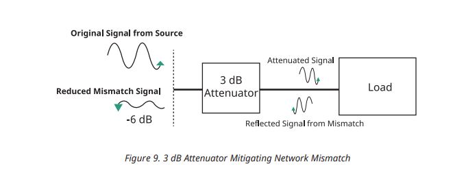 The MA245110A power sensor has the largest ALC input range of any similar power sensor that even with a fixed attenuator placed in-line between the VNA, the sensor would still manage the full swing of power levels from the VNA without any degradation of calibration.
Performance Overview
Performing a calibration from kHz frequencies up to 110 GHz can be done and with the Power Master MA24510A. Not only can this frequency plan be easily accomplished, with accuracy, industry leading level control, fast calibration time, but long-term stability are also benefits in the Anritsu Power Master MA24510A. There are other solutions on the market but the Power Master can deliver the most benefits with the lowest cost.
The following information will show how the Anritsu Power Master works with the Anritsu VectorStar VNA.
Test Setup and Procedure
The objective of the power calibration is to improve the accuracy of the power delivered to the DUT beyond what is provided by the default factory ALC calibrations.
Procedure:
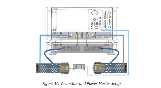
1. Have a 2- or 4-port 110 GHz ME7838A setup with all modules connected to the VectorStar base unit2. Attach the Power Master MA24510A to the front/rear USB ports on the VectorStar unit.
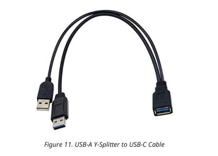
Note: The Power Master uses current greater than 500 mA, so a dual USB A cable to USB-C cable will need to be used (figure 11).
2. Attach the Power Master MA24510A to the front/rear USB ports on the VectorStar unit. 0Note: The Power Master uses current greater than 500 mA, so a dual USB A cable to USB-C cable will need to be used (figure 11).
3. The Power Master software will load and startup automatically on the ME7838A system upon connecting.
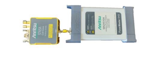
4. Connect the Power Master to the Port 1 mmWave module as shown below to perform Power calibration at source port.
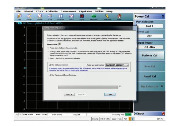
5. Navigate to the power calibration menu and set the desired target power which is required at the input of the device. Once the target power is entered and perform calibration is executed, a dialogue prompting the model number of Power Master along with its serial number will be displayed. Select start calibration to begin source power calibration.
6. After successful calibration of the source power, a message with the accuracy or max error will be displayed along with a message indicating the power calibration was successfully completed.
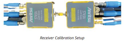
7. The calibrated power of the source should be transferred to the receiver. This process is called receiver calibration which transfers the power accuracy of the source to the receiver. This requires the two mmWave i.e., the source (port 1) and receive (port 2) modules to be connected with a W1 or 1 mm barrel adapter (Anritsu 33WW50, 33WWF50, 33WFWF50 adapter or similar) between connectors.
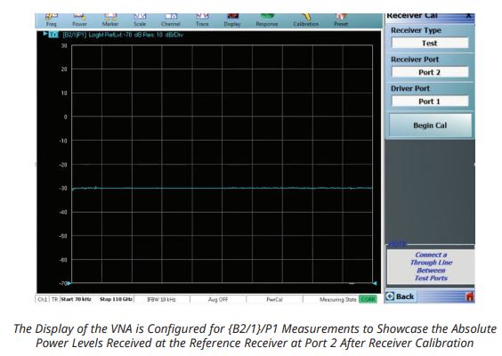
An example of -30 dBm of source power calibration followed by receiver calibration is shown in the below image


