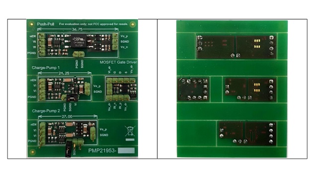
Description
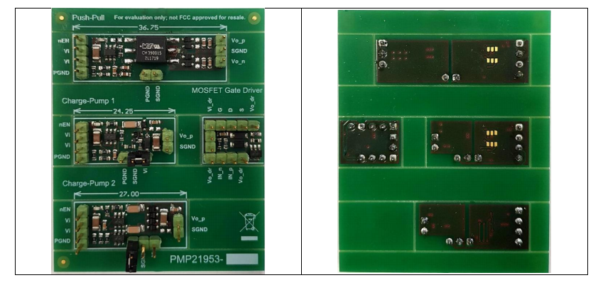
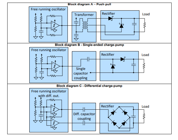
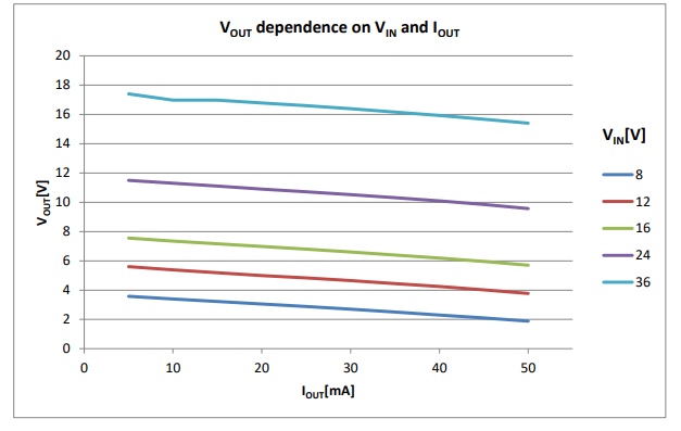
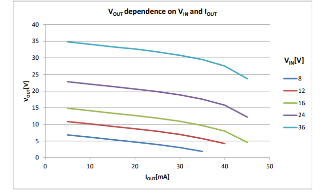
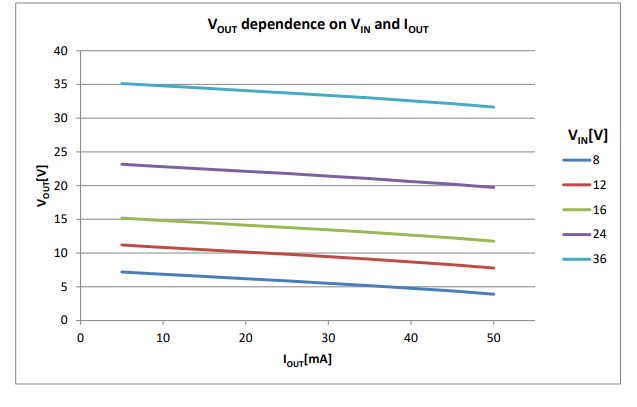
This reference design demonstrates a cost-focused approach of an isolated power supply with low current capability. The design consists of three options of three different topologies. All three design options are based on a high-voltage comparator TLV1805-Q1 which works as a free-running oscillator and a driver. There is no control loop, therefore, the output voltage depends on the input voltage and load.
Designs are intended to be used in automotive applications for example:
- Isolation amplifier supply for hot-side current sensing
- NFET reverse polarity protection charge pump
- Back-to-back NFET gate drive charge-pump (e.g. power disconnector)
- Small IGBT/SiC gate drive power supply
The features common to all three topologies:
- Automotive voltage input allows direct connection to the car battery (Vin_max=40V)
- Easy customizable for various applications
- Low BOM cost
- Tiny PCB area
Additionally, a simple output voltage limiter was designed single-ended charge-pump topology. Purpose of this is to statically drive a gate of a NFET while not exceeding VGS of the NFET even in case of the higher input voltage. This replaces using just a Zener diode. Use of this voltage limiter results in a significant decrease of static current consumption because the oscillator gets disabled as soon as the output voltage reaches the desired value. However, this creates a slow secondary voltage oscillations.
 1 Test Prerequisites
1.1 Voltage and Current Requirements
Table 1. Voltage and Current Requirements – topology A (Push-Pull)
| PARAMETER | SPECIFICATIONS |
| Input voltage | 8..36VDC |
| Output voltage | 4..18VDC |
| Output current | 5..50mA |
Table 2. Voltage and Current Requirements – topology B (Single-ended Charge-pump)
| PARAMETER | SPECIFICATIONS |
| Input voltage | 8..36VDC |
| Output voltage | 8..36VDC |
| Output current | 5..45mA |
Table 3. Voltage and Current Requirements – topology C (Single-ended Charge-pump)
| PARAMETER | SPECIFICATIONS |
| Input voltage | 8..36VDC |
| Output voltage | 8..36VDC |
| Output current | 5..50mA |
1.2 Required Equipment
- Regulated bench power supply
- Oscilloscope
- Electronic load
- Multimeters
1.3 Considerations
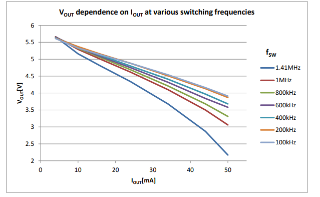
Push-pull switching frequency considerations have been done in order to find the best efficiency. Optimal frequency balances the use of transformer at higher voltages and switching losses.
Load regulation graph (below) shows the dependency of output voltage on load current for different various frequencies.
With regard to transformer saturation at the highest input voltage compromise frequency of around 300kHz was selected.
 2 Testing and Results
2.1 Efficiency Graphs
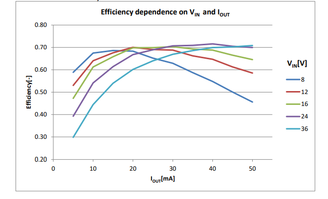
2.1.1 Topology A (Push-Pull)
- Iout between positive output and GND.
- Maximum efficiency: 72%
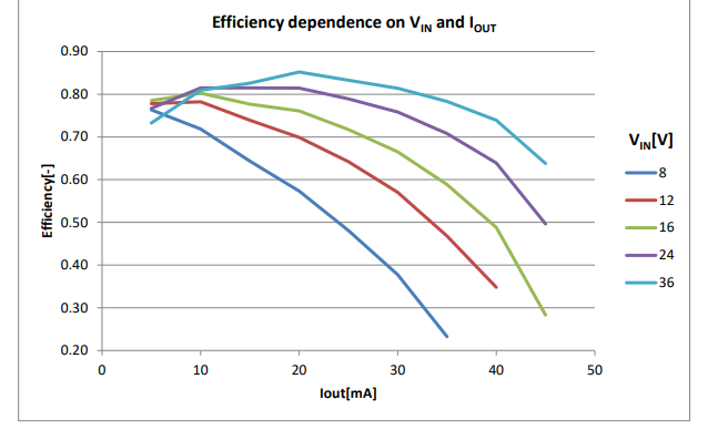
2.1.2 Topology B (Single-ended Charge-pump)
- Maximum efficiency: 85%
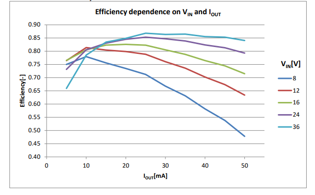
2.1.3 Topology C (Differential Charge-pump)
- Maximum efficiency: 87%
 2.2 Load regulation Graphs
2.2.1 Topology A (Push-Pull)
2.2.2 Topology B (Single-ended Charge-pump)
2.2.3 Topology C (Differential Charge-pump)
3 Waveforms
3.1 Start-up Sequence
3.1.1 Topology B (Single-ended Charge-pump), output voltage limiter not populated
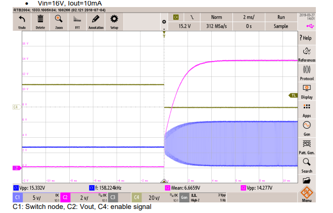
C1: Switch node, C2: Vout, C4: enable signal
3.1.2 Topology C (Single-ended Charge-pump)
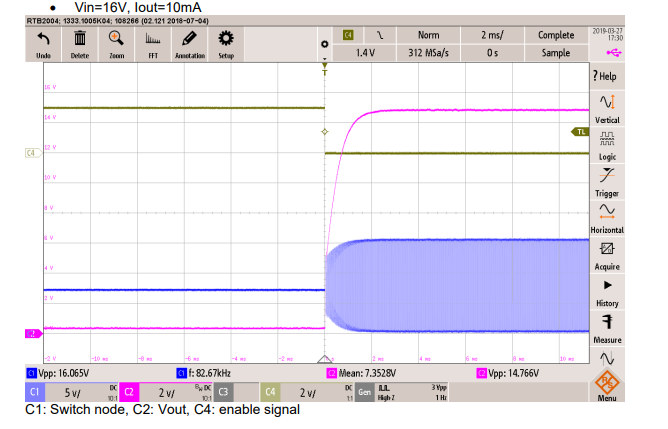 C1: Switch node, C2: Vout, C4: enable signal
3.2 Other
3.2.1 Topology B (Single-ended Charge-pump) output voltage limiter populated
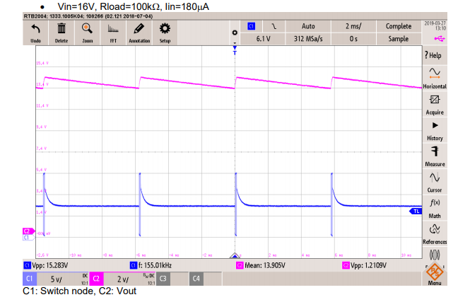 C1: Switch node, C2: Vout
Article Courtesy: Texas Instruments


