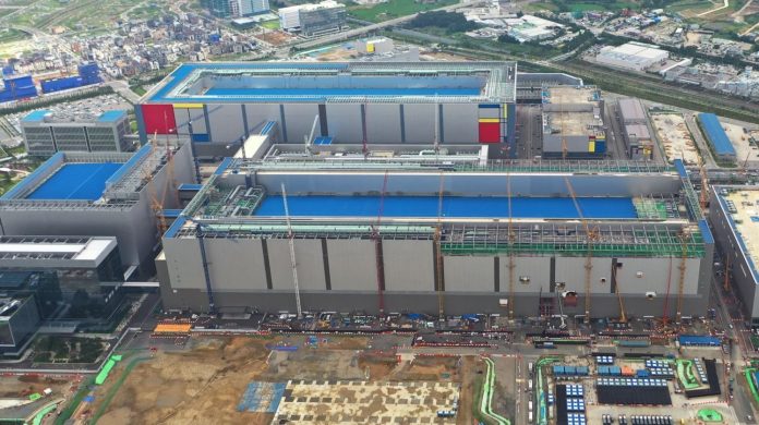
Samsung Electronics Co Ltd said it has begun mass producing chips with advanced 3-nanometre technology, the first to do so globally, as it seeks new clients to catch far bigger rival TSMC in contract chip manufacturing.
Compared with conventional 5-nanometre chips, the newly developed first-gen 3-nanometre process can reduce power consumption by up to 45%, improve performance by 23%, and reduce the area by 16%, Samsung said in a statement.
The South Korean firm did not name clients for its latest foundry technology, which supplies made-to-order chips like mobile processors and high-performance computing chips, and analysts said Samsung itself and Chinese companies are expected to be among the initial customers.
Taiwan Semiconductor Manufacturing Co (TSMC) is the world’s most advanced foundry chipmaker and controls about 54% of the global market for contract production of chips, used by firms such as Apple and Qualcomm which don’t have their own semiconductor facilities.
Samsung, a distant second with a 16.3% market share, according to data provider TrendForce, announced a 171 trillion won ($132 billion) investment plan last year to overtake TSMC as the world’s top logic chipmaker by 2030.
“We will continue active innovation in competitive technology development,” said Siyoung Choi, Head of Foundry Business at Samsung.
Samsung Co-CEO Kyung Kye-hyun said earlier this year its foundry business would look for new clients in China, where it expects high market growth, as companies from automakers to appliance goods manufacturers rush to secure capacity to address persistent global chip shortages.
While Samsung is the first to produce with 3-nanometre chip production, TSMC is planning 2-nanometre volume production in 2025.
Samsung is the market leader in memory chips, but it had been outspent by frontrunner TSMC in the more diverse foundry business, making it difficult to compete, analysts said.
“Non-memory is different, there’s too much variety,” said Kim Yang-jae, an analyst at Daol Investment & Securities.
“There are only two kinds of memory chips – DRAM and NAND Flash. You can concentrate on one thing, raise efficiency and make a lot of it, but you can’t do that with a thousand different non-memory chips.”
Samsung’s compound annual growth rate (CAGR) of capital spending between 2017 and 2023, which measures how quickly a company is increasing its investment, is estimated at 7.9%, versus TSMC’s estimated 30.4%, according to Mirae Asset Securities.
Samsung’s efforts to compete with the industry leader have also been hampered by less-than-expected yields of older chips during the past year or so, analysts said. The company said in March that its operations have shown a gradual improvement.


