The computers of the future could work almost at the speed of light and nanophotonics, the study of light at the nanometer scale, could be the key.
The Center for Integrated Nanostructure Physics (CINAP) within the Institute for Basic Science (IBS) has developed three key components of a circuit that works with light. Published in Nature Communications, these devices are designed to combine the advantages of photonics and electronics on the same platform.
While we are slowing approaching the end point of Moore’s Law: a state where we physically cannot shrink the dimension of our transistors much further. The future of big data processing requires high performance computers with higher speed operations.
Researchers reckon that if we build computers that process information through light rather than electrons, computer will be able to work faster. However, at nanometer dimensions, the wavelength of light is larger than the diameter of the silicon fiber making it difficult to control light’s propagation.
A solution to this problem can come from surface plasmons—electromagnetic waves that propagate along the surface of some conductive materials like silver, gold, aluminum and copper. Using surface plasmons, optical information can be transmitted nearly at the speed of light and in extremely miniature volumes.
Optical Transistors, Multiplexers and Signal Detectors
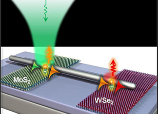
Using surface plasmons in silver nanowires and 2D semiconductors like molybdenum disulphide (MoS2), IBS researchers built three key components for optical communication: optical transistors, optical multiplexers and optical signal detectors.
These devices work thanks to a phenomenon called plasmon-exciton-plasmon interconversion.
The researchers constructed the optical transistor by interconnecting the silver nanowire to a flake of molybdenum disulfide (MoS2). Light shone on the device is converted to surface plasmon, then to exciton, then back to surface plasmon and eventually emitted as light with a shorter wavelength compared to the initial input. For example, if the input light is green, the output light can be red.
Wavelength multiplexing devices were realized in a similar way, but instead of having only a flake of MoS2, the researchers used an array of three different 2D semiconductor materials emitting light at different wavelengths. In this structure, for example, a single input light (violet color) generates three output lights (blue, green and red).
The propagating optical signals along the silver nanowire can be also transformed and detected as electrical signals by an optical signal detector.
“The originality of this paper arises from the exciton-plasmon interconversion. We published before the conversion of exciton to plasmon, and from plasmon to exciton using silver nanowire/2D semiconductor hybrids, but this is the first time that we can complete the circle going from plasmons to excitons and back to plasmons. Using this concept, we created optical transistors and multiplexors,” explained professor Hyun Seok Lee, first author of this study.


