As technology advances, so does the technology that is powering it. Over the years, a number of energy creation, energy storage, and energy harvesting devices have been developed to provide power to large electronic systems and individual electronic devices in a range of ways. As society moves towards Industry 4.0 and the Internet of Things (IoT), there’s an opportunity to create many types of ultra-small devices that can be used for automation and remote monitoring, and telemedicine applications.
Powering small-scale devices—especially in remote applications—requires unconventional self-powering mechanisms to be self-sufficient. In recent years, a number of different small-scale energy harvesters, known as nanogenerators, have gathered interest for powering small-scale devices in medical, remote monitoring, and IoT applications. The small size of these devices means they are not too bulky for the small devices they are powering. Despite their small size, they can still provide enough electricity for many devices to self-charge using their natural operating environment. In some cases, it might also be possible to use nanogenerators for large-scale harvesting—if many individual devices are integrated into a single harvesting system—however, this is something that has not been looked at yet from a widespread research perspective.
While there are a number of different nanogenerators, they are all used in different operating environments because the generation of an electrical charge is often governed by the stimuli in the surrounding environment. One of the more promising, widely talked about, and widely researched nanogenerators is the piezoelectric nanogenerator—often referred to in shorthand as a PENG.
Using the Piezoelectric Effect
PENGs use the piezoelectric effect to generate an electric charge. The piezoelectric effect is when an electrical charge is generated under an applied stress/load on a material. The piezoelectric effect is a reversible effect, so once the stress has been removed, the electrical charge stops. This also means that the piezoelectric effect can work in the other direction where an electrical voltage can be applied to the material, causing the atomic structure of the material to deform and become stress-induced.
In terms of the specific mechanisms, it is the rearrangement of ions at the atomic level—within the solid-state lattice—that generates the piezoelectricity. Most piezoelectric materials are inorganic in nature, and when they aren’t, they have some form of crystal structure (inorganic materials have this also). This means that (mostly) the piezoelectric has a regular and repeating array of well-ordered cations and anions within its atomic lattice. It is the deformation of the ions within this regularly patterned lattice that generates an electrical charge. While the material retains an overall neutral charge—the overall charge of the material doesn’t change, only the localized distribution of charges at the atomic level changes.
So, when the stress/load is applied to the piezoelectric material, the oppositely charged ions move from their original positions within the lattice to a point where they lie closer to each other. This rearrangement alters the charge balance within the lattice and induces an external electric field. The effects of the charge imbalance also permeate throughout the material. The result is the appearance of a net charge—either positive or negative—on one of the outer faces of the crystal. This subsequently creates a voltage across the oppositely charged crystal face. The piezoelectric charge can be harnessed, but when the stress stimulus is removed, the crystal lattice returns to its natural state and the voltage ceases.
In certain scenarios—such as the movement of a limb in wearable electronics, the movement of internal organs in implantable electronics, or the movement of the local surrounding environment in remote sensing/monitoring applications, to name a few—movements can create stresses across the piezoelectric material at the atomic scale that can then be harnessed.
In many cases where the PENG is used, the harnessing of the induced stress and the resulting electrical charge can then be used to power a small device that it is attached to. However, in certain situations—mainly sensing—the nanogenerator can act as both the powering device and the sensing device, as the generation of an electrical charge can act as a usable and detectable output for the sensor in load-bearing/stress-sensing situations.
Why 2D Materials Are Showing Promise for PENG Energy Harvesters
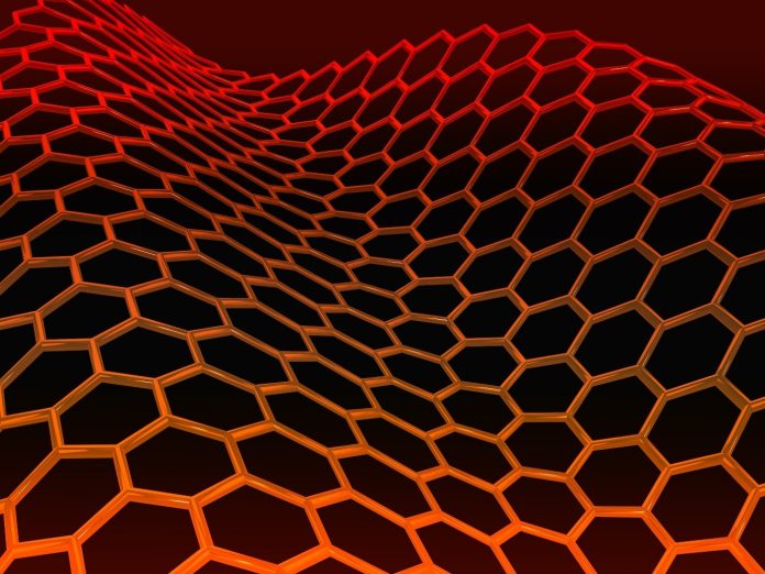
2D materials show promise for PENG Energy Harvesters for a number of reasons. First, the inherent thinness and small size of 2D materials enable the creation of ultra-small harvesting devices that are small enough to power the very small nodes in IoT systems, power very small sensors in remote monitoring applications, and charge small-scale implantable or wearable medical devices. By contrast, bulkier materials would create harvesting/power systems that are too large and unfeasible for these types of applications. This is why you often see nanomaterials touted for wearable/implantable electronics, IoT, and remote sensing applications.
Another aspect is the mechanical strength and flexibility of many 2D materials. Because the piezoelectric effect is induced by some level of mechanical deformation, the materials generating the electric current need to be robust and be able to withstand many bending cycles. The inherent thinness of 2D materials means that they have a very high degree of flexibility. While graphene has the highest flexibility, inorganic materials have relatively high flexibility compared to their bulkier counterparts, and other inorganic materials in general. When this flexibility is coupled with high mechanical strength, it means that the 2D materials can withstand a great deal of mechanical stress, leading to PENGs that can withstand many bending cycles, and in turn, be able to produce an electrical charge for longer time periods than when using other materials.
Then, there’s also the ability to exhibit piezoelectric properties. Traditionally, piezoelectric properties are seen in a range of inorganic materials, including natural and synthetic crystal materials, synthetic ceramics, group III-V and II-VI semiconductors, and various metal oxide complexes. Many different 2D materials are also known to exhibit piezoelectric properties, some of which are semiconducting materials. In terms of the materials of interest for PENGs, currently, hexagonal boron nitride (h-BN), various semiconducting transition metal dichalcogenides, group III and IV monochalcogenides, and chemically modified graphene—so that it is more semiconducting in nature rather than fully conducting as it naturally has no electronic bandgap—are the go-to choices.
Factors to Be Aware of with 2D Material PENGs
While the potential for creating PENGs using 2D materials exists, they, like any material, need to be used in the right way. In many cases, the piezoelectricity is only seen in single and few layered 2D materials. Once you get beyond this, the level of piezoelectricity generated is insufficient to power devices. As more 2D layers are added, this diminishing effect has been attributed to the lattice distortion caused by strain and the consequent charge polarization in the crystal. The more layers, the less flexible the 2D material is, so the lower the induced amount of strain, and therefore, the lower the degree of crystal polarization and generated electrical charge.
There have also been some other interesting phenomenon discovered with some 2D materials known as the layer dependence effect. While it’s not applicable to all 2D materials, it’s not only the number of layers that can influence the piezoelectric properties of the 2D material, but also whether there is an odd or even number of layers. This is because, in some cases, an odd number of layers has piezoelectric properties, but once the number of layers becomes even, the other layer becomes counterbalanced leading to piezoresistive properties. This then reverts to piezoelectric properties once another layer is added, and so forth until the layers become too great to exhibit piezoelectric properties anyway
Nevertheless, despite needing to ensure that the 2D materials are used in the correct manner, there are several 2D materials that can be harnessed, including a few materials where their bulkier 3D inorganic counterparts show no piezoelectric properties. There are now also many ways to create single and few layered 2D materials on a commercial level, so these kinds of challenges are not as significant as they would have been even just a few years ago. So, there’s a chance to break away from the traditional piezoelectric materials when it comes to creating these small-scale nanogenerators.
Conclusion
The piezoelectric effect is a common phenomenon in a range of bulk inorganic materials, but it is also observed in a range of 2D materials. 2D materials that can generate a piezoelectric charge that can be used in a range of PENGs for powering small-scale devices. There are a lot of benefits of using 2D materials in PENGs, including high flexibility and mechanical strength, as well as an inherent thinness, and PENGs offer a lot of potential for small-scale energy harvesting in remote applications—be it IoT, monitoring, or medical applications.


