Grain boundaries (GBs) in PSCs have been found to be detrimental to the photovoltaic performance of the devices. Numerous papers reported that the defects in perovskite GBs should be passivated by suitable materials, such as quaternary ammonium halide, fullerene derivatives, and CH3NH3I, to alleviate carrier recombination and consequently improve the device performance.
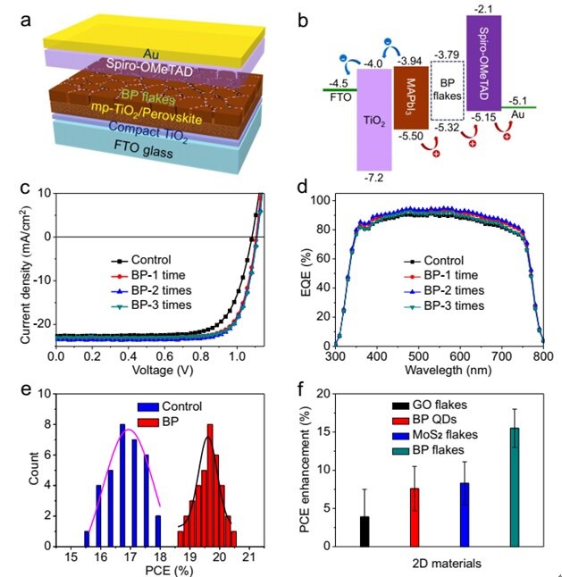
A team of scientists has developed a novel method to overcome the drawback of perovskite GBs without defect passivation on them. Several 2D materials, including black phosphorus (BP), MoS2, and graphene oxide (GO), are specifically modified on the edge of perovskite GBs by a solution process.
The 2D materials have high carrier mobilities, ultrathin thicknesses, and smooth surfaces without dangling bonds. The PCEs of the devices are substantially enhanced by the 2D flakes, in which BP flakes can induce the highest relative enhancement of about 15%. More interestingly, they find that, under certain conditions, GBs modified with the 2D materials are favorable for the device performance. Therefore, a synergistic effect between the 2D flakes and perovskite GBs is observed for the first time.
Although the nanotechnology of using 2D materials in PSCs has been reported in some papers, the synergistic effect between the 2D flakes and perovskite GBs has not been reported until now. To better understand the underlying mechanism of the above effect, device simulation was conducted by using commercial software. The hole conduction processes from GBs to 2D flakes in PSCs are clearly demonstrated, showing that the GBs and 2D flakes all act as hole channels in the devices.
The simulation results confirm that the performance enhancement induced by BP is higher than that of other 2D materials because of the highest hole mobility of BP. In addition, the modification of the 2D flakes on the perovskite grains away from GBs has little effect on the device performance, indicating that the synergistic effect of 2D flakes and perovskite GBs is essential to the performance enhancement in our devices.
Although the coverage of the 2D flakes on the perovskite films is only several percent, most of the flakes are located on perovskite GBs. Due to the high carrier mobilities of the 2D materials especially BP, hole transfer from GBs is dramatically enhanced in the PSCs, resulting in substantial improvements of the efficiency as well as the stability of the devices. These results also indicate that GBs in PSCs are not detrimental to the device performance if the accumulated holes in the GBs can be conducted out efficiently.
Under certain conditions, GBs even can be favorable for the photovoltaic performance of PSCs due to the built-in electric fields around them, which can facilitate photocarrier separation and transfer in the devices. Therefore, perovskite GBs are electrically benign, which is consistent with some theoretical calculations reported before. More importantly, they observed the synergic effect of the 2D flakes on the GBs in PSCs for the first time. Both the carrier mobility and the location of the 2D flakes on the perovskite surface are essential to the performance enhancement.
This work provides a guideline for modifying perovskite layers with novel high-mobility 2D materials to improve the photovoltaic performance as well as the stability of PSCs.

